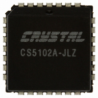
CS5102A-JLZ Cirrus Logic Inc, CS5102A-JLZ Datasheet - Page 15

CS5102A-JLZ
Manufacturer Part Number
CS5102A-JLZ
Description
IC ADC 16BIT 100/20KHZ 28-PLCC
Manufacturer
Cirrus Logic Inc
Datasheet
1.CS5101A-BL8Z.pdf
(39 pages)
Specifications of CS5102A-JLZ
Number Of Bits
16
Sampling Rate (per Second)
20k
Data Interface
Serial
Number Of Converters
1
Power Dissipation (max)
65mW
Voltage Supply Source
Analog and Digital, Dual ±
Operating Temperature
0°C ~ 70°C
Mounting Type
Surface Mount
Package / Case
28-PLCC
Lead Free Status / RoHS Status
Lead free / RoHS Compliant
Other names
598-1080-5
Available stocks
Company
Part Number
Manufacturer
Quantity
Price
Company:
Part Number:
CS5102A-JLZ
Manufacturer:
Cirrus Logic Inc
Quantity:
10 000
Part Number:
CS5102A-JLZ
Manufacturer:
CRYSTAL
Quantity:
20 000
2.
The CS5101A and CS5102A are 2-channel, 16-bit
A/D converters. The devices include an inherent
sample/hold and an on-chip analog switch for 2-
channel operation. Both channels can thus be
sampled and converted at rates up to 50 kSps
each (CS5101A) or 10 kSps each (CS5102A). Al-
ternatively, each of the devices can be operated as
a single channel ADC operating at 100 kSps
(CS5101A) or 20 kSps (CS5102A).
Both the CS5101A and CS5102A can be config-
ured to accept either unipolar or bipolar input rang-
es, and data is output serially in either binary or 2's
complement coding. The devices can be config-
ured in 3 different output modes, as well as an in-
ternal,
CS5101A
charge/fine charge control, to allow accurate track-
ing of high-slew signals.
3.
The CS5101A and CS5102A implement the suc-
cessive approximation algorithm using a charge
redistribution architecture. Instead of the traditional
resistor network, the DAC is an array of binary-
weighted capacitors. All capacitors in the array
share a common node at the comparator's input.
DS45F6
A G N D
V R E F
A IN
OVERVIEW
THEORY OF OPERATION
synchronous
+
+
+
-
-
-
and
Figure 3. Coarse Charge Input Buffers & Charge Redistribution DAC
CS5102A
Fine
C o arse
Fine
C o a rse
Fine
C o a rse
loopback
C
Bit 15
M S B
provide
mode.
C /2
C
to t
Bit 14
coarse
= C + C /2 + C /4 + C /8 + ... C /3 2 ,7 68
The
C /4
Bit 13
As shown in Figure 3, their other terminals are ca-
pable of being connected to AGND, VREF, or AIN
(1 or 2). When the device is not calibrating or con-
verting, all capacitors are tied to AIN. Switch S1 is
closed and the charge on the array, tracks the in-
put signal.
When the conversion command is issued, switch
S1 opens. This traps the charge on the comparator
side of the capacitor array and creates a floating
node at the comparator's input. The conversion al-
gorithm operates on this fixed charge, and the sig-
nal at the analog input pin is ignored. In effect, the
entire DAC capacitor array serves as analog mem-
ory during conversion much like the hold capacitor
in a sample/hold amplifier.
The conversion consists of manipulating the free
plates of the capacitor array to VREF and AGND to
form a capacitive divider. Since the charge at the
floating node remains fixed, the voltage at that
point depends on the proportion of capacitance
tied to VREF versus AGND. The successive ap-
proximation algorithm is used to find the proportion
of capacitance, which when connected to the refer-
ence will drive the voltage at the floating node to
zero. That binary fraction of capacitance repre-
sents the converter's digital output.
C /3 2 ,7 6 8
Bit 0
LSB
C /3 2 ,7 6 8
CS5101A CS5102A
D u m m y
S1
+
-
15


