ADC12441CIJ National Semiconductor, ADC12441CIJ Datasheet
ADC12441CIJ
Specifications of ADC12441CIJ
Available stocks


Related parts for ADC12441CIJ

ADC12441CIJ Summary of contents
Page 1
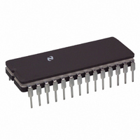
... Connection Diagram ADC12441CMJ ADC12441CMJ 883 See NS Package Number J28A TL H 11017 – 1 November 1994 12 bits plus sign (max (min (max) b 100 ns 100 ps rms 1 LSB (max LSB (max (max) 55 kHz (max) Dual-In-Line Package TL H 11017 – 2 Top View Order Number or ADC12441CIJ RRD-B30M115 Printed ...
Page 2
... REF C Analog Input Capacitance IN DYNAMIC CHARACTERISTICS Bipolar Effective Bits (Note 17) Unipolar Effective Bits (Note 17 Bipolar Signal-to-Noise Ratio (Note 17 Unipolar Signal-to-Noise Ratio (Note 17) Operating Ratings (Notes 1 2) Temperature Range ADC12441CIJ ADC12441CMJ ADC12441CMJ 883 and AV Voltage (Notes 3V Negative Supply Voltage (V Reference Voltage 0 3V) ...
Page 3
Converter Electrical Characteristics The following specifications apply for V CC Impedance 600 and MHz unless otherwise specified Boldface limits apply for CLK all other limits (Notes 6 7 and 8) ...
Page 4
Digital and DC Electrical Characteristics The following specifications apply for DV CC otherwise specified Boldface limits apply for T (Notes 6 and 7) (Continued) Symbol Parameter I TRI-STATE Output Leakage OUT Current I Output Source Current SOURCE I Output Sink ...
Page 5
AC Electrical Characteristics Note 4 The power dissipation of this device under normal operation should never exceed 169 mW (Quiescent Power Dissipation outputs) Caution should be taken not to exceed absolute maximum power rating when the device is operating in ...
Page 6
Electrical Characteristics (Continued) FIGURE 1b Simplified Error Curve vs Output Code without Auto-Cal or Auto-Zero Cycles FIGURE 1c Simplified Error Curve vs Output Code after Auto-Cal Cycle Typical Performance Characteristics Zero Error vs V REF TL H 11017– 6 Zero ...
Page 7
Typical Performance Characteristics Linearity Error vs V REF Bipolar Signal-to- Noise Distortion Ratio vs a Input Frequency Bipolar Signal-to- Noise Distortion Ratio vs a Input Signal Level Bipolar Spectral Response with 1 kHz Sine Wave Input (Continued) Linearity Error vs ...
Page 8
Typical Performance Characteristics Bipolar Spectral Response with 20 kHz Sine Wave Input Test Circuits FIGURE 2 TRI-STATE Test Circuits and Waveforms Timing Diagrams Auto-Cal Cycle (CS (Continued) Unipolar Spectral Response with 20 kHz Sine Wave Input TL H 11017– 10 ...
Page 9
Timing Diagrams (Continued) Normal Conversion with Auto-Zero (CAL Normal Conversion without Auto-Zero (CAL 11017– 11017– 18 ...
Page 10
Pin Descriptions DV (28) CC The digital and analog positive power supply AV (4) CC pins The digital and analog power supply voltage range of the ADC12441 guarantee accuracy it is required a that ...
Page 11
Functional Description Digital Control Inputs CAL FIGURE 1 Function of the A D Control Inputs The table in Figure 1 ...
Page 12
Analog Considerations For absolute accuracy where the analog input varies be- tween very specific voltage limits the reference pin can be biased with a time and temperature stable voltage source In general the magnitude of the reference voltage ...
Page 13
Dynamic Performance Many applications require the A D converter to digitize ac signals but the standard dc integral and differential nonlin- earity specifications will not accurately predict the A D con- verter’s performance with ac input signals The ...
Page 14
... Physical Dimensions inches (millimeters) Order Number ADC12441CMJ ADC12441CMJ 883 or ADC12441CIJ LIFE SUPPORT POLICY NATIONAL’S PRODUCTS ARE NOT AUTHORIZED FOR USE AS CRITICAL COMPONENTS IN LIFE SUPPORT DEVICES OR SYSTEMS WITHOUT THE EXPRESS WRITTEN APPROVAL OF THE PRESIDENT OF NATIONAL SEMICONDUCTOR CORPORATION As used herein 1 Life support devices or systems are devices or ...