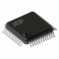
TDA8784HL/C4,151 NXP Semiconductors, TDA8784HL/C4,151 Datasheet - Page 5

TDA8784HL/C4,151
Manufacturer Part Number
TDA8784HL/C4,151
Description
IC ADC 10BIT 18MSPS 48-LQFP
Manufacturer
NXP Semiconductors
Type
ADCr
Datasheet
1.TDA8784HLC4518.pdf
(28 pages)
Specifications of TDA8784HL/C4,151
Package / Case
48-LQFP
Resolution (bits)
10 b
Sampling Rate (per Second)
18M
Data Interface
Serial
Voltage Supply Source
Analog and Digital
Voltage - Supply
4.75 V ~ 5.25 V
Operating Temperature
-20°C ~ 75°C
Mounting Type
Surface Mount
Product
Analog Front End
Interface Type
Serial (3-Wire)
Supply Voltage (max)
5.25 V
Supply Voltage (min)
2.5 V, 4.75 V
Supply Current
1 mA, 18 mA, 78 mA
Maximum Operating Temperature
+ 75 C
Minimum Operating Temperature
- 20 C
Mounting Style
SMD/SMT
Number Of Channels
1
Lead Free Status / RoHS Status
Lead free / RoHS Compliant
Other names
568-3607
935266802151
TDA8784HLBE-S
935266802151
TDA8784HLBE-S
Available stocks
Company
Part Number
Manufacturer
Quantity
Price
Company:
Part Number:
TDA8784HL/C4,151
Manufacturer:
NXP Semiconductors
Quantity:
10 000
Philips Semiconductors
PINNING
2002 Oct 23
CLPOB
AGND4
OFDOUT
AMPOUT
AGND1
V
AGCOUT
CPCDS
AGND5
ADCIN
CLPADC
V
DACOUT
AGND2
V
V
V
DEC1
AGND6
SDATA
SCLK
SEN
STDBY
V
DGND1
D0
D1
D2
D3
D4
D5
D6
D7
D8
D9
OGND
SYMBOL
CCA1
ref
CCA2
RB
RT
CCD1
18 Msps, 10-bit analog-to-digital
interface for CCD cameras
PIN
10
11
12
13
14
15
16
17
18
19
20
21
22
23
24
25
26
27
28
29
30
31
32
33
34
35
36
1
2
3
4
5
6
7
8
9
clamp pulse input at optical black
analog ground 4
analog output of the additional 8-bit control DAC (controlled via the serial interface)
CDS amplifier output (fixed gain = 6 dB)
analog ground 1
analog supply voltage 1
AGC amplifier signal output
clamp storage capacitor pin
analog ground 5
ADC analog signal input from AGCOUT via a short circuit
clamp control input for ADC analog input signal clamp (used with a capacitor from V
ADC input clamp reference voltage (normally connected to pin V
ground via a capacitor)
DAC output for ADC clamp level
analog ground 2
analog supply voltage 2
ADC reference voltage (BOTTOM) code 0
ADC reference voltage (TOP) code 1023
decoupling 1 (decoupled to ground via a capacitor)
analog ground 6
serial data input for the 4 control DACs (9-bit DAC for AGC gain, 8-bit DAC for frequency cut-off;
additional 8-bit DAC for OFD output voltage; 10-bit DAC for ADC clamp level and the standby mode
per block and edge pulse control); see Fig.3, Fig.4 and Table 1
serial clock input for the control DACs and their serial interface; see Fig.3, Fig.4 and Table 1
enable input for the serial interface shift register (active when SEN = logic 0); see Fig.3, Fig.4 and
Table 1
standby control (active HIGH); all the output bits are logic 0 when standby is enabled
digital supply voltage 1
digital ground 1
ADC digital output 0 (LSB)
ADC digital output 1
ADC digital output 2
ADC digital output 3
ADC digital output 4
ADC digital output 5
ADC digital output 6
ADC digital output 7
ADC digital output 8
ADC digital output 9 (MSB)
digital output ground
5
DESCRIPTION
RB
or DACOUT, or connected to
Product specification
TDA8784
ref
to ground)


