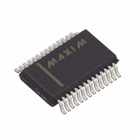
MAX1407CAI+ Maxim Integrated Products, MAX1407CAI+ Datasheet - Page 19

MAX1407CAI+
Manufacturer Part Number
MAX1407CAI+
Description
IC DAS 16BIT LP 28-SSOP
Manufacturer
Maxim Integrated Products
Type
Data Acquisition System (DAS)r
Datasheet
1.MAX1409CAP.pdf
(48 pages)
Specifications of MAX1407CAI+
Resolution (bits)
16 b
Sampling Rate (per Second)
60
Data Interface
Serial
Voltage Supply Source
Analog and Digital
Voltage - Supply
2.7 V ~ 3.6 V
Operating Temperature
0°C ~ 70°C
Mounting Type
Surface Mount
Package / Case
28-SSOP
Number Of Converters
1
Resolution
16 bit
Interface Type
Serial (4-Wire, SPI, QSPI, Microwire)
Supply Voltage (max)
3.6 V
Supply Voltage (min)
2.7 V
Maximum Power Dissipation
762 mW
Maximum Operating Temperature
+ 70 C
Mounting Style
SMD/SMT
Minimum Operating Temperature
0 C
Lead Free Status / RoHS Status
Lead free / RoHS Compliant
When used in unbuffered mode, the switched capacitor
sampling front end of the modulator presents a dynam-
ic load to the driving circuitry. The size of the internal
sampling capacitor and the input sampling frequency
(Figure 6) determines the dynamic load (see Dynamic
Input Impedance section). As the gain increases, the
input sampling capacitance also increases. Since the
MAX1407/MAX1408/MAX1409/MAX1414 sample at a
constant rate for all gain settings, the dynamic load pre-
sented by the inputs varies with the gain setting.
An integrated programmable-gain amplifier (PGA) pro-
vides three user-selectable gains: +1/3V/V, +1V/V, and
+2V/V to maximize the dynamic range of the ADC. Bits
GAIN1 and GAIN0 set the desired gain (see ADC
Register). The gain of +1/3V/V allows the direct mea-
surement of the supply voltage through an internal mul-
tiplexer input or through an auxillary input.
The MAX1407/MAX1408/MAX1409/MAX1414 perform
analog-to-digital conversions using a single-bit, sec-
ond-order, switched-capacitor delta-sigma modulator.
The delta-sigma modulation converts the input signal
into a digital pulse train whose average duty cycle rep-
resents the digitized signal information. The pulse train
is then processed by a digital decimation filter.
The modulator provides 2nd-order frequency shaping
of the quantization noise resulting from the single bit
quantizer. The modulator is fully differential for maxi-
mum signal-to-noise ratio and minimum susceptibility to
power-supply noise. The modulator operates at one of
two different sampling rates resulting in an output data
rate of either 30Hz or 60Hz (see ADC Register).
Figure 6. Analog Input—Unbuffered Mode
R
EXT
C
EXT
Low-Power, 16-Bit Multichannel DAS with
Internal Reference,10-Bit DACs, and RTC
______________________________________________________________________________________
C
R
PIN
MUX
C
ST
R
SW
C
SAMPLE
ADC Modulator
Unbuffered Mode
PGA Gain
C
C
The MAX1407/MAX1408/MAX1409/MAX1414 are capa-
ble of performing digital offset correction to eliminate
changes due to power-supply voltage or system tem-
perature. At the end of a calibration cycle, a 16-bit cali-
bration value is stored in the Offset register in two’s
compliment format. After completing a conversion, the
MAX1407/MAX1408/MAX1409/MAX1414 subtract the
calibration value from the ADC conversion result and
write the offset compensated data to the Data register
(see Offset Register section). Either a positive or nega-
tive offset can be calibrated. During offset calibration,
DRDY will go high. DRDY goes low after calibration is
complete. The offset register can be programmed to
skew the ADC offset with a maximum range from -2
(+2
value is +2LSB (-2LSB), this translates to a -2LSB
(+2LSB) shift in bipolar mode or a -4LSB (+4LSB) shift in
unipolar mode.To maintain optimum performance, recal-
ibrate the ADC if the temperature changes by more than
20°C. Offset calibration should also be performed after
any changes in PGA gain, bipolar/unipolar input range,
buffered/unbuffered mode, or conversion speed. During
calibration, the two mulitplexers will be disabled and the
inputs to the ADC will internally be shorted to a com-
mon-mode voltage.
The on-chip digital filter processes the 1-bit data
stream from the modulator using a SINC
The SINC
settling time is 3/60Hz or 50ms (for RATE bit in ADC
register set to 1) and 3/30Hz or 100ms (for RATE bit set
to “0”).
The transfer function for a SINC
three cascaded SINC
the Z-domain by:
and in the frequency domain by:
where N, the decimation factor, is the ratio of the modu-
lator frequency f
15
- 1)LSBs, e.g., if the programmed 2’s complement
3
filters settle in three data word periods. The
ADC Digital Filter Characteristics
H ƒ
H z
( )
( )
M
=
to the output frequency f
=
N
1
1
N
1
sin
filters. This can be described in
sin
(
(
1
1
ADC Offset Calibration
−
−
N
z
π
z
π
−
−
ƒ
N
1
ƒ
ƒ
M
)
ƒ
)
3
M
ADC Digital Filter
filter function is that of
3
3
3
filter function.
N
.
15
19
to


