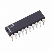
LTC1094ACN Linear Technology, LTC1094ACN Datasheet - Page 21

LTC1094ACN
Manufacturer Part Number
LTC1094ACN
Description
IC DATA ACQ SYS 10BIT 8CH 20-DIP
Manufacturer
Linear Technology
Type
Data Acquisition System (DAS), ADCr
Datasheet
1.LTC1091CN8PBF.pdf
(32 pages)
Specifications of LTC1094ACN
Resolution (bits)
10 b
Data Interface
Serial
Voltage Supply Source
Dual ±
Voltage - Supply
4.5 V ~ 10 V
Operating Temperature
-40°C ~ 85°C
Mounting Type
Through Hole
Package / Case
20-DIP (0.300", 7.62mm)
Lead Free Status / RoHS Status
Contains lead / RoHS non-compliant
Sampling Rate (per Second)
-
Available stocks
Company
Part Number
Manufacturer
Quantity
Price
Company:
Part Number:
LTC1094ACN
Manufacturer:
TI
Quantity:
7 818
Part Number:
LTC1094ACN
Manufacturer:
LT/凌特
Quantity:
20 000
3. Analog Inputs
Because of the capacitive redistribution A/D conversion
techniques used, the analog inputs of the LTC1091/
LTC1092/LTC1093/LTC1094 have capacitive switching
input current spikes. These current spikes settle quickly
and do not cause a problem. However, if large source
resistances are used or if slow settling op amps drive the
inputs, care must be taken to ensure that the transients
caused by the current spikes settle completely before the
conversion begins.
Source Resistance
The analog inputs of the LTC1091/LTC1092/LTC1093/
LTC1094 look like a 60pF capacitor (C
500
switched between the selected “+” and “–” inputs once
during each conversion cycle. Large external source resis-
tors and capacitances will slow the settling of the inputs. It
is important that the overall RC time constants be short
enough to allow the analog inputs to completely settle
within the allowed time.
“+” Input Settling
This input capacitor is switched onto the “+” input during
the sample phase (t
is the 1 1/2 CLK cycles before the conversion starts. The
voltage on the “+” input must settle completely within this
sample time. Minimizing R
the input settling time. If large “+” input source resistance
must be used, the sample time can be increased by using
a slower CLK frequency. With the minimum possible
sample time of 3 s, R
provide adequate settling.
A
PPLICATI
resistor (R
O
ON
SMPL
U
) as shown in Figure 7. C
S
SOURCE
, see Figure 8). The sample phase
I FOR ATIO
U
SOURCE
+
< 2k and C1 < 20pF will
+
and C1 will improve
W
IN
) in series with a
U
IN
gets
V
V
IN
IN
+
–
0.5mV/DIV
0.5mV/DIV
R
R
Figure 7. Analog Input Equivalent Circuit
SOURCE
SOURCE
Figure 5. Poor V
Noise and Ripple Can Cause A/D Errors
Figure 6. Good V
Noise and Ripple on V
+
–
C1
INPUT
INPUT
C2
“+”
“–”
LTC1093/LTC1094
LTC1091/LTC1092
10 s/DIV
10 s/DIV
CC
CC
Bypassing.
Bypassing Keeps
3RD CLK
4TH CLK
CC
Below 1mV
R
ON
= 500
LTC1091
1091-4 F05
1091-4 F06
C
60pF
LTC091-4 F07
IN
=
21


