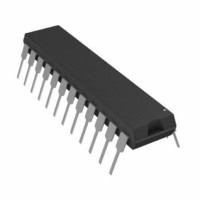
AD7890BN-10 Analog Devices Inc, AD7890BN-10 Datasheet - Page 17

AD7890BN-10
Manufacturer Part Number
AD7890BN-10
Description
IC DAS 12BIT 8CH 24-DIP
Manufacturer
Analog Devices Inc
Type
Data Acquisition System (DAS)r
Datasheet
1.AD7890ARZ-10.pdf
(28 pages)
Specifications of AD7890BN-10
Mounting Type
Through Hole
Package / Case
24-DIP (0.300", 7.62mm)
Rohs Status
RoHS non-compliant
Resolution (bits)
12 b
Sampling Rate (per Second)
117k
Data Interface
Serial
Voltage Supply Source
Single Supply
Voltage - Supply
±10V
Operating Temperature
-40°C ~ 85°C
Supply Voltage
5V
No. Of Bits
12 Bit
Interface Type
Serial
Lead Free Status / RoHS Status
SERIAL INTERFACE
The AD7890’s serial communications port provides a flexible
arrangement to allow easy interfacing to industry-standard
microprocessors, microcontrollers, and digital signal processors.
A serial read to the AD7890 accesses data from the output
register via the DATA OUT line. A serial write to the AD7890
writes data to the control register via the DATA IN line.
Two different modes of operation are available, optimized for
different types of interface where the AD7890 can act either as
master in the system (it provides the serial clock and data
framing signal) or acts as slave (an external serial clock and
framing signal can be provided to the AD7890). The former is
self-clocking mode while the latter is external clocking mode.
SELF-CLOCKING MODE
The AD7890 is configured for its self-clocking mode by tying
the SMODE pin of the device to a logic low. In this mode, the
AD7890 provides the serial clock signal and the serial data
DATA OUT (O)
DATA IN (I)
SCLK (O)
SCLK (O)
RFS (O)
TFS (I)
THREE-STATE
t
NOTES:
1. (I) SIGNIFIES AN INPUT.
2. (O) SIGNIFIES AN OUTPUT. PULL-UP RESISTOR ON SCLK.
9
t
8
A2
t
2
t
NOTES:
1. (I) SIGNIFIES AN INPUT.
2. (O) SIGNIFIES AN OUTPUT. PULL-UP RESISTOR ON SCLK.
1
LEADING
ZERO
t
10
A1
t
11
Figure 11. Self-Clocking (Master) Mode Control Register Write
Figure 10. Self-Clocking (Master) Mode Output Register Read
A2
A0
t
3
A1
t
3
CONV
Rev. C | Page 17 of 28
A0
t
4
STBY
t
framing signal used for the transfer of data from the AD7890.
This self-clocking mode can be used with processors that allow
an external device to clock their serial port, including most
digital signal processors.
Read Operation
Figure 10 shows a timing diagram for reading from the AD7890
in the self-clocking mode. At the end of conversion, RFS goes
low and the serial clock (SCLK) and serial data (DATA OUT)
outputs become active. Sixteen bits of data are transmitted with
one leading zero, followed by the three address bits of the
control register, followed by the 12-bit conversion result starting
with the MSB. Serial data is clocked out of the device on the
rising edge of SCLK and is valid on the falling edge of SCLK.
The RFS output remains low for the duration of the 16 clock
cycles. On the 16
high and DATA OUT is disabled.
4
DB11
DON’T
CARE
t
5
DB10
th
DON’T
CARE
rising edge of SCLK, the RFS output is driven
t
12
DB0
t
6
t
DON’T
CARE
7
THREE-STATE
AD7890


