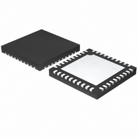
MAX1359BETL+ Maxim Integrated Products, MAX1359BETL+ Datasheet - Page 35

MAX1359BETL+
Manufacturer Part Number
MAX1359BETL+
Description
IC DAS 16BIT 40-TQFN
Manufacturer
Maxim Integrated Products
Type
Data Acquisition System (DAS)r
Specifications of MAX1359BETL+
Resolution (bits)
16 b
Sampling Rate (per Second)
21.84k
Data Interface
Serial
Voltage Supply Source
Analog and Digital
Voltage - Supply
1.8 V ~ 3.6 V
Operating Temperature
-40°C ~ 85°C
Mounting Type
Surface Mount
Package / Case
40-TQFN Exposed Pad
Number Of Converters
2
Resolution
16 bit
Interface Type
Serial (4-Wire, SPI, QSPI, Microwire)
Voltage Reference
1.25 V
Supply Voltage (max)
3.6 V
Supply Voltage (min)
1.8 V
Maximum Power Dissipation
2051.3 mW
Maximum Operating Temperature
+ 85 C
Mounting Style
SMD/SMT
Input Voltage
1.8 V to 3.6 V
Minimum Operating Temperature
- 40 C
Lead Free Status / RoHS Status
Lead free / RoHS Compliant
Table 6. Setting the ADC Conversion Rate*
The actual rates are:
*Calculate the ADC sampling rate using the following
equation:
where f
CONTINUOUS
CONVERSION
UPIOs, RTC, Voltage Monitors, and Temp Sensor
RATE (sps)
CONTINUOUS
CONVERSION
16-Bit, Data-Acquisition System with ADC, DAC,
RATE (sps)
NOMINAL
200
240
400
512
10
40
50
60
HFCLK
200
240
400
512
10
40
50
60
= 4.9152MHz nominally.
f
S
CONVERSION
=
RATE (sps)
______________________________________________________________________________________
SINGLE
448
12.5
100
128
2.5
10
15
50
60
DECIMATION
×
decimation ratio
RATIO
1096
274
220
183
f
HFCLK
55
46
27
23
RATE2
0
0
0
0
1
1
1
1
RATE1
CONTINUOUS
CONVERSION
10.01042142
40.04168568
49.87009943
199.4803977
238.5091712
406.3489583
477.0183424
RATE (sps)
59.953125
0
0
1
1
0
0
1
1
ACTUAL
RATE0
0
1
0
1
0
1
0
1
-RATE<2:0>: ADC conversion-rate-setting bits. These
three bits set the conversion rate of the ADC as shown
in Table 6. The initial conversion requires four conver-
sion cycles for valid data and subsequent conversions
require only one cycle (if CONT = 1). A full-scale input
change can require up to five cycles for valid data if
the digital filter is not reset with the STRT or S bit.
MODE<2:0>: Conversion-mode bits. These three bits
determine the type of conversion for the ADC as shown
in Table 7. When the ADC finishes an offset calibration
and/or gain calibration, the MODE<2:0> bits clear to 0
hex, the ADD bit in the STATUS register asserts, and
an interrupt asserts on INT (or UPIO_ if programmed as
DRDY) if MADD is unmasked. Perform a gain calibra-
tion after achieving the desired offset (calibrated or
not). If an offset and gain calibration are performed
together (MODE<2:0> = 7 hex), the offset calibration is
performed first followed by the gain calibration, and the
µC is interrupted by INT (or UPIO_ if programmed as
DRDY) if MADD is unmasked only upon completion of
both offset and gain calibration. After power-on or cali-
bration, the ADC does not begin conversions until initi-
ated by the user (see the ADCE and STRT bit
descriptions in this section and see the S bit descrip-
tions in the MUX Register section). See the GAIN CAL
Register and OFFSET CAL Register sections for details
on system calibration.
Table 7. Setting the ADC Conversion Mode
Normal
System Offset Calibration
System Gain Calibration
Normal
Normal
Self Offset Calibration
Self Gain Calibration
Self Offset and Gain
Calibration
CONVERSION MODE
MODE2
0
0
0
0
1
1
1
1
MODE1
0
0
1
1
0
0
1
1
MODE0
0
1
0
1
0
1
0
1
35


