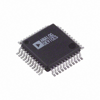
AD7891AS-2 Analog Devices Inc, AD7891AS-2 Datasheet - Page 8

AD7891AS-2
Manufacturer Part Number
AD7891AS-2
Description
IC DAS 12BIT 8CH 44-MQFP
Manufacturer
Analog Devices Inc
Type
Data Acquisition System (DAS)r
Datasheet
1.AD7891BSZ-2.pdf
(20 pages)
Specifications of AD7891AS-2
Rohs Status
RoHS non-compliant
Resolution (bits)
12 b
Sampling Rate (per Second)
500k
Data Interface
Serial, Parallel
Voltage Supply Source
Single Supply
Voltage - Supply
5V
Operating Temperature
-40°C ~ 85°C
Mounting Type
Surface Mount
Package / Case
44-MQFP, 44-PQFP
Available stocks
Company
Part Number
Manufacturer
Quantity
Price
Company:
Part Number:
AD7891AS-2
Manufacturer:
AD
Quantity:
1 831
Part Number:
AD7891AS-2
Manufacturer:
ADI/亚德诺
Quantity:
20 000
AD7891
SERIAL INTERFACE MODE FUNCTIONS
When the part is configured for serial mode (MODE = 0), five of the 12 data input/output lines provide serial interface functions.
These functions are outlined below.
PLCC Pin No. MQFP Pin No. Mnemonic
18
15
16
21
17
13, 14
CONTROL REGISTER
The control register for the AD7891 contains six bits of information as described below. These six bits can be written to the control
register either in a parallel mode write operation or via a serial mode write operation. The default (power-on) condition of all bits in
the control register is 0. Six serial clock pulses must be provided to the part in order to write data to the control register. If TFS
returns high before six serial clock cycles, no data transfer takes place to the control register and the write cycle has to be restarted to
write data to the control register. However, if the SWCONV bit of the register was previously set to a Logic 1 and TFS is brought
high before six serial clock cycles, another conversion is initiated.
A2
A1
A0
SWCONV
SWSTBY
FORMAT
12
9
10
15
11
7, 8
Address Input. This input is the most significant address input for multiplexer channel selection.
Address Input. This is the second most significant address input for multiplexer channel selection.
Address Input. Least significant address input for multiplexer channel selection. When the address is written to
the control register, an internal pulse is initiated to allow for the multiplexer settling time and track/hold acquisi-
tion time before the track/hold goes into hold and conversion is initiated. When the internal pulse times out, the
track/hold goes into hold and conversion is initiated. The selected channel is given by the formula
Conversion Start. Writing a 1 to this bit initiates a conversion in a similar manner to the CONVST input. Con-
tinuous conversion starts do not take place when there is a 1 in this location. The internal pulse and the conver-
sion process are initiated when a 1 is written to this bit. With a 1 in this bit, the hardware conversion start, i.e.,
the CONVST input, is disabled. Writing a 0 to this bit enables the hardware CONVST input.
Standby Mode Input. Writing a 1 to this bit places the device in its standby or power-down mode. Writing a 0 to
this bit places the device in its normal operating mode.
Data Format. Writing a 0 to this bit sets the conversion data output format to straight (natural) binary. This
data format is generally used for unipolar input ranges. Writing a 1 to this bit sets the conversion data output
format to twos complement. This output data format is generally used for bipolar input ranges.
SCLK
TFS
RFS
DATA OUT
DATA IN
TEST
A
2
A
1
A
A
0
2
¥
S
4
Serial Clock Input. This is an externally applied serial clock that is used to
load serial data to the control register and to access data from the
output register.
Transmit Frame Synchronization Pulse. Active low logic input with serial
data expected after the falling edge of this signal.
Receive Frame Synchronization Pulse. This is an active low logic input
with RFS provided externally as a strobe or framing pulse to access serial data
from the output register. For applications that require that data be transmitted
and received at the same time, RFS and TFS should be connected together.
Serial Data Output. Sixteen bits of serial data are provided with the
data FORMAT bit and the three address bits of the control register
preceding the 12 bits of conversion data. Serial data is valid on the falling
edge of SCLK for 16 edges after RFS goes low. Output conversion data
coding is twos complement when the FORMAT bit of the control register is
1 and straight binary when the FORMAT bit of the control register is 0.
Serial Data Input. Serial data to be loaded to the control register is provided
at this input. The first six bits of serial data are loaded to the control
register on the first six falling edges of SCLK after TFS goes low. Serial
data on subsequent SCLK edges is ignored while TFS remains low.
Test Pin. When the device is configured for serial mode of operation,
two of the pins which had been data inputs become test inputs. To ensure
correct operation of the device, both TEST inputs should be tied to a
logic low potential.
W
Description
+
C
A
O
–8–
1 2
N
¥
V
+
S
A
W
0
S
+
T
1
B
Y
L
F
S
O
B
R
(
M
D
A
B
T
) 0
REV. D


