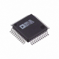
AD7891BS-1 Analog Devices Inc, AD7891BS-1 Datasheet

AD7891BS-1
Specifications of AD7891BS-1
Related parts for AD7891BS-1
AD7891BS-1 Summary of contents
Page 1
FEATURES Fast 12-Bit ADC with 1.6 s Conversion Time 8 Single-Ended Analog Input Channels Overvoltage Protection on Each Channel Selection of Input Ranges for AD7891 +2 2.5 V ...
Page 2
AD7891–SPECIFICATIONS Parameter 2 DYNAMIC PERFORMANCE 4 Signal-to-(Noise + Distortion) Ratio @ 25∞ MIN MAX 4 Total Harmonic Distortion 4 Peak Harmonic or Spurious Noise 4 Intermodulation Distortion Second-Order Terms Third-Order Terms 4 Channel-to-Channel Isolation DC ACCURACY Resolution ...
Page 3
Parameter A Version LOGIC OUTPUTS Output High Voltage, V 4.0 OH Output Low Voltage, V 0.4 OL DB11to DB0 ± 10 Floating-State Leakage Current 5 Floating-State Capacitance 15 Output Coding Straight (Natural) Binary CONVERSION RATE Conversion Time 1.6 Track/Hold Acquisition ...
Page 4
AD7891 TIMING CHARACTERISTICS Parameter Versions t 1.6 CONV Parallel Interface ...
Page 5
... Model Input Range AD7891ACHIPS-1 AD7891ACHIPS-2 ± ± AD7891AS-1 ± ± AD7891ASZ-1 ± ± AD7891AP-1 ± ± AD7891AP-1REEL ± ± AD7891BS-1 ± ± AD7891BP-1 ± ± AD7891BP-1REEL ± ± AD7891YS-1 ± ± AD7891YS-1REEL ± ± AD7891YP-1 ± ± AD7891YP-1REEL +2.5 V, ± 2.5 V AD7891AS +2.5 V, ± ...
Page 6
AD7891 PLCC MQFP Pin No. Pin No. Mnemonic 1–5 28– INXA INXB 34– AGND 20 14 DGND STANDBY REF OUT/REF ...
Page 7
PLCC Pin No. MQFP Pin No. Mnemonic Data I/O Lines There are 12 data input/output lines on the AD7891. When the part is configured for parallel ...
Page 8
AD7891 SERIAL INTERFACE MODE FUNCTIONS When the part is configured for serial mode (MODE = 0), five of the 12 data input/output lines provide serial interface functions. These functions are outlined below. PLCC Pin No. MQFP Pin No. Mnemonic 18 ...
Page 9
TERMINOLOGY Signal-to-(Noise + Distortion) Ratio This is the measured ratio of signal to (noise + distortion) at the output of the ADC. The signal is the rms amplitude of the fundamental. Noise is the rms sum of all nonfundamental signals ...
Page 10
AD7891 CONVERTER DETAILS The AD7891 is an 8-channel, high speed, 12-bit data acquisi- tion system. It provides the user with signal scaling, multiplexer, track/hold, reference, ADC, and high speed parallel and serial interface logic functions on a single chip. The ...
Page 11
Serial Interface Mode The serial interface mode is selected by tying the MODE input to a logic low. In this case, five of the data/control inputs of the parallel mode assume serial interface functions. The serial interface on the AD7891 ...
Page 12
AD7891 CIRCUIT DESCRIPTION Reference The AD7891 contains a single reference pin labeled REF OUT/ REF IN that either provides access to the part’s own 2.5 V internal reference or to which an external 2.5 V reference can be connected to ...
Page 13
Table I. Ideal Code Transition Table for the AD7891-1, Analog Input Input Voltage 2 3 +FSR /2 – 3/2 LSB (9.99268 V, 4.99634 V or 2.49817 V) +FSR/2 – 5/2 LSB (9.98779 V, 4.99390 V or 2.49695 V) +FSR/2 – ...
Page 14
AD7891 Track/Hold Amplifier The track/hold amplifier on the AD7891 allows the ADC to accurately convert an input sine wave of full-scale amplitude to 12-bit accuracy. The input bandwidth of the track/hold is greater than the Nyquist rate of the ADC ...
Page 15
As in the 8X51 circuit in Figure 7, the way the 68HC11 is informed that a conversion is completed is not shown in the diagram. The EOC line can be used to inform the 68HC11 that a conversion is complete ...
Page 16
AD7891 PARALLEL INTERFACING The parallel port on the AD7891 allows the device to be interfaced to microprocessors or DSP processors as a memory mapped or I/O mapped device. The CS and RD inputs are common to all memory peripheral interfacing. ...
Page 17
AD7891 to DSP5600x Figure 15 shows a parallel interface between the AD7891 and the DSP5600x series of DSPs. The AD7891 should be mapped into the top 64 locations of Y data memory. If extra wait states are needed in this ...
Page 18
AD7891 AD7891 PERFORMANCE Linearity The linearity of the AD7891 is primarily determined by the on-chip 12-bit DAC. This is a segmented DAC that is laser trimmed for 12-bit integral linearity and differential linearity. Typical INL for the AD7891 is ± ...
Page 19
Effective Number of Bits The formula for signal-to-(noise + distortion) ratio (see Terminology section) is related to the resolution or number of bits of the converter. Rewriting the formula gives a measure of performance expressed in effective number of bits ...
Page 20
AD7891 2.10 2.00 1.95 0.25 MIN VIEW A ROTATED 90 CCW Revision History Location 4/04—Data Sheet changed from REV REV. D. Changes to SPECIFICATIONS . . . . . . . . . . . . . . ...


