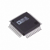
AD7891YS-1 Analog Devices Inc, AD7891YS-1 Datasheet - Page 13

AD7891YS-1
Manufacturer Part Number
AD7891YS-1
Description
IC DAS 12BIT 8CH 44-MQFP
Manufacturer
Analog Devices Inc
Type
Data Acquisition System (DAS)r
Datasheet
1.AD7891BSZ-2.pdf
(20 pages)
Specifications of AD7891YS-1
Rohs Status
RoHS non-compliant
Resolution (bits)
12 b
Sampling Rate (per Second)
500k
Data Interface
Serial, Parallel
Voltage Supply Source
Single Supply
Voltage - Supply
5V
Operating Temperature
-55°C ~ 105°C
Mounting Type
Surface Mount
Package / Case
44-MQFP, 44-PQFP
Analog Input
+FSR
+FSR – 5/2 LSB
+FSR – 7/2 LSB
AGND + 5/2 LSB
AGND + 3/2 LSB
AGND + 1/2 LSB
NOTES
1
2
3
4
Analog Input
+FSR
+FSR/2 – 5/2 LSB
+FSR/2 – 7/2 LSB
AGND + 3/2 LSB
AGND + 1/2 LSB
AGND – 1/2 LSB
AGND – 3/2 LSB
–FSR/2 + 5/2 LSB
–FSR/2 + 3/2 LSB
–FSR/2 + 1/2 LSB
NOTES
1
2
3
4
Transfer Function of the AD7891-1 and AD7891-2
The transfer function of the AD7891-1 and AD7891-2 can be
expressed as
D is the output data from the AD7891 and is in the range 0 to
4095 for straight binary encoding and from –2048 to +2047 for
twos complement encoding. Values for M depend upon the
input voltage range. Values for N depend upon the input voltage
range and the output data format. These values are given in
Table III. REF IN is the reference voltage applied to the AD7891.
REV. D
Output code format is determined by the FORMAT bit in the control register.
FSR is the full-scale range and is 5 V for the 0 to 5 V range and 2.5 V for the 0 to 2.5 V range, with REF IN = 2.5 V.
1 LSB = F
0 V to 5 V range or 0 V to 2.5 V range.
Output code format is determined by the FORMAT bit in the control register.
FSR is full-scale range and is +20 V for the ± 10 V range, +10 V for the ± 5 V range, and +5 V for the ± 2.5 V range, with REF IN = +2.5 V.
1 LSB = FSR/4096 = +4.88 mV (± 10 V range), +2.44 mV (± 5 V range), and +1.22 mV (± 2.5 V range), with REF IN = +2.5 V.
± 10 V range, ± 5 V range, or ± 2.5 V range.
Input Voltage
2
2
/2 – 3/2 LSB
– 3/2 LSB
Table I. Ideal Code Transition Table for the AD7891-1,
S
/4096 = 1.22 mV (0 to 5 V range) or 610 mV (0 to 2.5 V range), with REF IN = 2.5 V.
=
3
(
M
Table II. Ideal Code Transition Table for the AD7891-2, 0 V to 5 V and 0 V to 2.5 V Ranges
3
¥
REF IN
Input Voltage
(9.99268 V, 4.99634 V or 2.49817 V)
(9.98779 V, 4.99390 V or 2.49695 V)
(9.99145 V, 4.99146 V or 2.49573 V)
(7.3242 mV, 3.6621 mV or 1.8310 mV)
(2.4414 mV, 1.2207 mV or 0.6103 mV)
(–2.4414 mV, –1.2207 mV or –0.6103 mV)
(–7.3242 mV, –3.6621 mV or –1.8310 mV)
(–9.98779 V, –4.99390 V or –2.49695 V)
(–9.99268 V, –4.99634 V or –2.49817 V)
(–9.99756 V, –4.99878 V or –2.49939 V)
Input Voltage
(4.99817 V or 2.49908 V)
(4.99695 V or 2.49847 V)
(4.99573 V or 2.49786 V)
(3.0518 mV or 1.52588 mV)
(1.83105 mV or 0.9155 mV)
(0.6103 mV or 0.3052 mV)
¥
D
/4096
)
+
(
N
¥
REF IN
4
)
–13–
4
10 V and
Range
AD7891-1
± 10 V
± 10 V
± 5 V
± 5 V
AD7891-2
0 V to +5 V
0 V to +5 V
0 V to +2.5 V
0 V to +2.5 V
± 2.5 V
± 2.5 V
Twos Complement
011...110 to 011...111
011...101 to 011...110
011...100 to 011...101
100...010 to 000...011
100...001 to 000...010
100...000 to 000...001
Digital Output Code Transition
Table III. Transfer Function M and N Values
Twos Complement
011...110 to 011...111
011...101 to 011...110
011...100 to 011...101
000...001 to 000...010
000...000 to 000...001
111...111 to 000...000
111...110 to 111...111
100...010 to 100...011
100...001 to 100...010
100...000 to 100...001
5 V Ranges and the AD7891-2,
Digital Output Code Transition
Output Data Format
Straight Binary
Twos Complement
Straight Binary
Twos Complement
Straight Binary
Twos Complement
Straight Binary
Twos Complement
Straight Binary
Twos Complement
Straight Binary
111...110 to 111...111
111...101 to 111...110
111...100 to 111...101
100...001 to 100...010
100...000 to 100...001
011...111 to 100...000
011...110 to 011...111
000...010 to 000...011
000...001 to 000...010
000...000 to 000...001
Straight Binary
111...110 to 111...111
111...101 to 111...110
111...100 to 111...101
000...010 to 000...011
000...001 to 000...010
000...000 to 000...001
1
2.5 V Range
M
8
8
4
4
2
2
1
1
2
2
AD7891
1
N
–4
0
–2
0
0
1
0
0.5
–1
0


