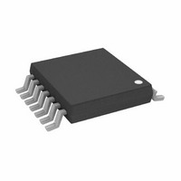
AD5252BRUZ1 Analog Devices Inc, AD5252BRUZ1 Datasheet - Page 22

AD5252BRUZ1
Manufacturer Part Number
AD5252BRUZ1
Description
IC DGTL POT DUAL 1K I2C 14-TSSOP
Manufacturer
Analog Devices Inc
Datasheet
1.AD5252BRUZ10.pdf
(28 pages)
Specifications of AD5252BRUZ1
Taps
256
Resistance (ohms)
1K
Number Of Circuits
2
Temperature Coefficient
650 ppm/°C Typical
Memory Type
Non-Volatile
Interface
I²C, 2-Wire Serial
Voltage - Supply
2.7 V ~ 5.5 V, ±2.25 V ~ 2.75 V
Operating Temperature
-40°C ~ 85°C
Mounting Type
Surface Mount
Package / Case
14-TSSOP
Resistance In Ohms
1.00K
End To End Resistance
1kohm
Track Taper
Linear
Resistance Tolerance
± 30%
No. Of Steps
256
Supply Voltage Range
2.7V To 5.5V, ± 2.25V To ± 2.75V
Control Interface
I2C, Serial
Lead Free Status / RoHS Status
Lead free / RoHS Compliant
For Use With
AD5252EVAL - BOARD EVAL FOR AD5252
Lead Free Status / RoHS Status
Lead free / RoHS Compliant, Lead free / RoHS Compliant
Available stocks
Company
Part Number
Manufacturer
Quantity
Price
Part Number:
AD5252BRUZ1
Manufacturer:
ADI/亚德诺
Quantity:
20 000
Company:
Part Number:
AD5252BRUZ10
Manufacturer:
Renesas
Quantity:
41
Part Number:
AD5252BRUZ10
Manufacturer:
ADI/亚德诺
Quantity:
20 000
Company:
Part Number:
AD5252BRUZ100
Manufacturer:
Analog Devices Inc
Quantity:
135
Company:
Part Number:
AD5252BRUZ100
Manufacturer:
ADI
Quantity:
3 529
AD5251/AD5252
DIGITAL INPUT/OUTPUT CONFIGURATION
SDA is a digital input/output with an open-drain MOSFET that
requires a pull-up resistor for proper communication. On the
other hand, SCL and WP are digital inputs for which pull-up
resistors are recommended to minimize the MOSFET cross-
conduction current when the driving signals are lower than
V
Figure 35
WP can be permanently tied to V
the write-protect feature is not used. If WP is left floating, an
internal current source pulls it low to enable write protection. In
applications in which the device is programmed infrequently,
this allows the part to default to write-protection mode after
any one-time factory programming or field calibration without
using an on-board pull-down resistor. Because there are
protection diodes on all inputs, the signal levels must not be
greater than V
MULTIPLE DEVICES ON ONE BUS
The AD5251/AD5252 are equipped with two addressing pins,
AD1 and AD0, that allow up to four AD5251/AD5252 devices
to be operated on one I
AD1 and AD0 on each device must first be defined. An example
is shown in Table 12 and Figure 37. In I
device is issued a different slave address—01011(AD1)(AD0)—
to complete the addressing.
DD
. SCL and WP have ESD protection diodes, as shown in
and
SCL
WP
Figure 36
DD
Figure 36. Equivalent WP Digital Input
to prevent forward biasing of the diodes.
Figure 35. SCL Digital Input
INPUTS
2
C bus. To achieve this result, the states of
.
GND
GND
DD
without a pull-up resistor if
2
V
V
C programming, each
DD
DD
Rev. B | Page 22 of 28
Table 12. Multiple Devices Addressing
AD1
0
0
1
1
TERMINAL VOLTAGE OPERATION RANGE
The AD5251/AD5252 are designed with internal ESD diodes
for protection; these diodes also set the boundaries for the
terminal operating voltages. Positive signals present on
Terminal A, Terminal B, or Terminal W that exceed V
clamped by the forward-biased diode. Similarly, negative signals
on Terminal A, Terminal B, or Terminal W that are more
negative than V
users should not operate V
the voltage across V
polarity constraint.
POWER-UP AND POWER-DOWN SEQUENCES
Because the ESD protection diodes limit the voltage compliance
at Terminal A, Terminal B, and Terminal W (see Figure 38), it is
important to power on V
these terminals. Otherwise, the diodes are forward biased such
that V
user’s circuit. Similarly, V
The ideal power-up sequence is in the following order: GND,
V
V
they are powered after V
DD
A
MASTER
, V
, V
B
DD
, V
SS
Figure 37. Multiple AD5251/AD5252 Devices on a Single Bus
Figure 38. Maximum Terminal Voltages Set by V
, digital inputs, and V
/V
W
, and the digital inputs is not important, as long as
SS
SDA SCL
AD1
AD0
are powered unintentionally and may affect the
AD0
0
1
0
1
R
SS
U1
P
are also clamped (see Figure 38). In practice,
DD
5V
to V
R
P
DD
DD
SDA SCL
AD1
AD0
DD
AB
/V
SS
/V
Device Addressed
U1
U2
U3
U4
/V
, V
5V
, but V
U2
SS
A
SS
SS
/V
.
WA
before applying any voltage to
should be powered down last.
, and V
B
/V
AB
5V
W
, V
SDA SCL
AD1
AD0
. The order of powering
WA
WB
U3
, and V
to be higher than
V
A
W
V
B
SS
DD
5V
DD
SDA
AD1
AD0
WB
and V
have no
SCL
U4
DD
SS
are
SDA
SCL


