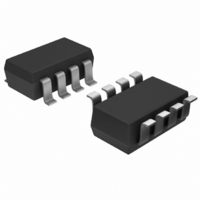
AD5245BRJZ5-R2 Analog Devices Inc, AD5245BRJZ5-R2 Datasheet - Page 16

AD5245BRJZ5-R2
Manufacturer Part Number
AD5245BRJZ5-R2
Description
IC DGTL POT 256POS SOT-23-8 T/R
Manufacturer
Analog Devices Inc
Datasheet
1.AD5245BRJZ100-RL7.pdf
(20 pages)
Specifications of AD5245BRJZ5-R2
Taps
256
Resistance (ohms)
5K
Number Of Circuits
1
Temperature Coefficient
45 ppm/°C Typical
Memory Type
Volatile
Interface
I²C, 2-Wire Serial
Voltage - Supply
2.7 V ~ 5.5 V
Operating Temperature
-40°C ~ 125°C
Mounting Type
Surface Mount
Package / Case
SOT-23-8
Resistance In Ohms
5K
End To End Resistance
5kohm
No. Of Steps
256
Resistance Tolerance
± 30%
Supply Voltage Range
2.7V To 5.5V
Control Interface
I2C, Serial
No. Of Pots
Single
Lead Free Status / RoHS Status
Lead free / RoHS Compliant
For Use With
AD5245EVAL - BOARD EVAL FOR AD5245
Lead Free Status / RoHS Status
Lead free / RoHS Compliant, Lead free / RoHS Compliant
Other names
AD5245BRJZ5-R2
AD5245BRJZ5-R2TR
AD5245BRJZ5-R2TR
Available stocks
Company
Part Number
Manufacturer
Quantity
Price
Company:
Part Number:
AD5245BRJZ5-R2
Manufacturer:
AD
Quantity:
11 560
AD5245
I
I
The 2-wire I
1. The master initiates data transfer by establishing a START
2. In write mode, the second byte is the instruction byte.
2
2
C-COMPATIBLE 2-WIRE SERIAL BUS
C INTERFACE
condition, which is when a high-to-low transition on the SDA
line occurs while SCL is high (see Figure 45). The next byte
is the slave address byte, which consists of the 7-bit slave
address followed by an R/ W bit (this bit determines whether
data is read from or written to the slave device). The AD5245
has one configurable address bit, AD0 (see Table 8).
The slave whose address corresponds to the transmitted
address responds by pulling the SDA line low during the
ninth clock pulse (this is termed the acknowledge bit). At
this stage, all other devices on the bus remain idle while the
selected device waits for data to be written to or read from
its serial register. If the R/ W bit is high, the master reads
from the slave device. On the other hand, if the R/ W bit is
low, the master writes to the slave device.
The first bit (MSB) of the instruction byte is a don’t care.
The second MSB, RS, is the midscale reset. A logic high on
this bit moves the wiper to the center tap, where R
This feature effectively overwrites the contents of the
register; therefore, when taken out of reset mode, the RDAC
remains at midscale.
The third MSB, SD, is a shutdown bit. A logic high causes an
open circuit at Terminal A while shorting the wiper to
Terminal B. This operation yields almost 0 Ω in rheostat mode
or 0 V in potentiometer mode. It is important to note that
the shutdown operation does not disturb the contents of the
register. When brought out of shutdown, the previous setting is
applied to the RDAC. Also during shutdown, new settings can
be programmed. When the part is returned from shutdown,
the corresponding VR setting is applied to the RDAC.
The remainder of the bits in the instruction byte are don’t
cares (see Table 8).
2
C serial bus protocol operates as follows:
WA
= R
WB
Rev. B | Page 16 of 20
.
3. After acknowledging the instruction byte, the last byte in
4. In read mode, the data byte follows immediately after the
5. After all data bits have been read or written, a STOP
write mode is the data byte. Data is transmitted over the
serial bus in sequences of nine clock pulses (eight data bits
followed by an acknowledge bit). The transitions on the
SDA line must occur during the low period of SCL and
remain stable during the high period of SCL (see Figure 45).
acknowledgment of the slave address byte. Data is
transmitted over the serial bus in sequences of nine clock
pulses (a slight difference with write mode, in which eight
data bits are followed by an acknowledge bit). Similarly, the
transitions on the SDA line must occur during the low
period of SCL and remain stable during the high period of
SCL (see Figure 46).
condition is established by the master. A STOP condition is
defined as a low-to-high transition on the SDA line while
SCL is high. In write mode, the master pulls the SDA line
high during the 10
condition (see Figure 45). In read mode, the master issues a
no acknowledge for the ninth clock pulse (that is, the SDA
line remains high). The master then brings the SDA line low
before the 10
STOP condition (see Figure 46).
A repeated write function gives the user flexibility to update
the RDAC output a number of times after addressing and
instructing the part only once. For example, after the RDAC
has acknowledged its slave address and instruction bytes in
the write mode, the RDAC output updates on each successive
byte. If different instructions are needed, then the write/read
mode has to start again with a new slave address, instruction,
and data byte. Similarly, a repeated read function of the
RDAC is also allowed.
th
clock pulse, which goes high to establish a
th
clock pulse to establish a STOP


