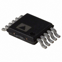
AD5243BRMZ100 Analog Devices Inc, AD5243BRMZ100 Datasheet - Page 5

AD5243BRMZ100
Manufacturer Part Number
AD5243BRMZ100
Description
IC DGTL POT DUAL 100K I2C 10MSOP
Manufacturer
Analog Devices Inc
Datasheet
1.AD5243BRMZ2.5.pdf
(20 pages)
Specifications of AD5243BRMZ100
Temperature Coefficient
35 ppm/°C Typical
Taps
256
Resistance (ohms)
100K
Number Of Circuits
2
Memory Type
Volatile
Interface
I²C, 2-Wire Serial
Voltage - Supply
2.7 V ~ 5.5 V
Operating Temperature
-40°C ~ 125°C
Mounting Type
Surface Mount
Package / Case
10-MSOP, Micro10™, 10-uMAX, 10-uSOP
Resistance In Ohms
100K
End To End Resistance
100kohm
No. Of Steps
256
Resistance Tolerance
± 20%
Supply Voltage Range
2.7V To 5.5V
Control Interface
Serial, I2C, 2-Wire
No. Of Pots
Dual
Number Of Elements
2
# Of Taps
256
Resistance (max)
100KOhm
Power Supply Requirement
Single
Interface Type
Serial (2-Wire/I2C)
Single Supply Voltage (typ)
3/5V
Dual Supply Voltage (typ)
Not RequiredV
Single Supply Voltage (min)
2.7V
Single Supply Voltage (max)
5.5V
Dual Supply Voltage (min)
Not RequiredV
Dual Supply Voltage (max)
Not RequiredV
Operating Temp Range
-40C to 125C
Operating Temperature Classification
Automotive
Mounting
Surface Mount
Pin Count
10
Lead Free Status / RoHS Status
Lead free / RoHS Compliant
For Use With
AD5243EVAL - BOARD EVAL FOR AD5243
Lead Free Status / Rohs Status
Compliant
Available stocks
Company
Part Number
Manufacturer
Quantity
Price
Part Number:
AD5243BRMZ100
Manufacturer:
ADI/亚德诺
Quantity:
20 000
Part Number:
AD5243BRMZ100-RL7
Manufacturer:
ADI/亚德诺
Quantity:
20 000
TIMING CHARACTERISTICS: ALL VERSIONS
V
Table 3.
Parameter
I
1
2
2
See the timing diagrams for the locations of measured values (that is, see Figure 3 and Figure 46 to Figure 49).
The maximum t
C INTERFACE TIMING CHARACTERISTICS
DD
SCL Clock Frequency
Bus-Free Time Between Stop and Start, t
Hold Time (Repeated Start), t
Low Period of SCL Clock, t
High Period of SCL Clock, t
Setup Time for Repeated Start Condition, t
Data Hold Time, t
Data Setup Time, t
Fall Time of Both SDA and SCL Signals, t
Rise Time of Both SDA and SCL Signals, t
Setup Time for Stop Condition, t
= 5 V ± 10%, or 3 V ± 10%; V
SCL
SDA
HD:DAT
P
must be met only if the device does not stretch the low period (t
HD;DAT
SU;DAT
t
1
2
S
LOW
HIGH
t
2
HD;STA
SU;STO
A
= V
t
3
DD
1
F
; V
BUF
R
t
8
SU;STA
B
t
8
= 0 V; −40°C < T
t
Figure 3. I
9
Symbol
f
t
t
t
t
t
t
t
t
t
t
SCL
1
2
3
4
5
6
7
8
9
10
t
6
2
C Interface Detailed Timing Diagram
t
4
t
Rev. A | Page 5 of 20
9
A
< +125°C; unless otherwise noted.
Conditions
After this period, the first clock pulse is
generated.
LOW
t
) of the SCL signal.
7
S
t
5
t
2
Min
0
1.3
0.6
1.3
0.6
0.6
100
0.6
AD5243/AD5248
Typ
P
t
10
Max
400
0.9
300
300
Unit
kHz
μs
μs
μs
μs
μs
μs
ns
ns
ns
μs


