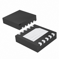
DS1841N+T&R Maxim Integrated Products, DS1841N+T&R Datasheet - Page 15

DS1841N+T&R
Manufacturer Part Number
DS1841N+T&R
Description
IC RES LOG NV I2C 10-TDFN
Manufacturer
Maxim Integrated Products
Datasheet
1.DS1841NTR.pdf
(17 pages)
Specifications of DS1841N+T&R
Taps
128
Resistance (ohms)
22K
Number Of Circuits
1
Temperature Coefficient
250 ppm/°C Typical
Memory Type
Non-Volatile
Interface
I²C, 2-Wire Serial
Voltage - Supply
2.7 V ~ 5.5 V
Operating Temperature
-40°C ~ 100°C
Mounting Type
Surface Mount
Package / Case
10-TDFN Exposed Pad
Resistance In Ohms
22K
Lead Free Status / RoHS Status
Lead free / RoHS Compliant
Writing multiple bytes to a slave: I
of multiple bytes can also be performed. During a sin-
gle write sequence, up to 8 bytes in one page can be
written at one time. If more than eight bytes are trans-
mitted in the sequence, then only the last eight trans-
mitted bytes are stored. After the last physical memory
location in a particular page (8-byte page write), the
address counter automatically wraps back to the first
location in the same page for subsequent byte write
operations.
Acknowledge polling: Any time a EEPROM byte is
written, the DS1841 requires the EEPROM write time
(t
the byte to EEPROM. During the EEPROM write time,
the device does not acknowledge its slave address
because it is busy. It is possible to take advantage of
this phenomenon by repeatedly addressing the
DS1841, which allows communication to continue as
soon as the DS1841 is ready. The alternative to
acknowledge polling is to wait for a maximum period of
t
Reading a single byte from a slave: Unlike the write
operation that uses the specified memory address byte
to define where the data is to be written, the read opera-
tion occurs at the present value of the memory address
Figure 4. I
W
W
A)
B)
C)
D)
TYPICAL I
EXAMPLE I
to elapse before attempting to access the device.
) after the STOP condition to write the contents of
START
SINGLE-BYTE WRITE
-WRITE CONTROL
REGISTER 0 TO 00h
SINGLE-BYTE READ
-READ TEMPERATURE
REGISTER
TWO-BYTE WRITE
- WRITE LUT VALUES FOR
REGISTERS 80h AND 81h
TWO-BYTE READ
- READ LUT REGISTERS
80h AND 81h
2
C WRITE TRANSACTION
2
MSB
C TRANSACTIONS (WHEN A0 AND A1 ARE CONNECTED TO GND)
2
0
C Communication Examples
1
0
ADDRESS*
SLAVE
______________________________________________________________________________________
1
0
START
START
START 0 1 0 1 0 0 0 0
START 0 1 0 1 0 0 0 0
A1
0 1 0 1 0 0 0 0
0 1 0 1 0 0 0 0
A0
50h
50h
50h
50h
READ/
WRITE
R/W
LSB
SLAVE
ACK
2
Temperature-Controlled, NV, I
SLAVE
SLAVE
SLAVE
SLAVE
C write operations
ACK
ACK
ACK
ACK
MSB
b7
0 0 0 0 0 0 1 0
0 0 0 0 1 1 0 0
1 0 0 0 0 0 0 0
1 0 0 0 0 0 0 0
b6
0Ch
02h
80h
80h
b5
REGISTER ADDRESS
*THE SLAVE ADDRESS IS DETERMINED BY ADDRESS PINS A0 AND A1.
b4
SLAVE
SLAVE
SLAVE
SLAVE
ACK
ACK
ACK
ACK
b3
0 0 0 0 0 0 0 0
0 1 0 0 0 0 0 0
REPEATED
REPEATED
b2
START
START
40h
counter. To read a single byte from the slave, the master
generates a START condition, writes the slave address
byte with R/W = 1, reads the data byte with a NACK to
indicate the end of the transfer, and generates a STOP
condition. However, since requiring the master to keep
track of the memory address counter is impractical, the
following method should be used to perform reads from
a specified memory location.
Reading multiple bytes from a slave: The read opera-
tion can be used to read multiple bytes with a single
transfer. When reading bytes from the slave, the master
simply ACKs the data byte if it desires to read another
byte before terminating the transaction. After the master
reads the last byte it must NACK to indicate the end of
the transfer and generates a STOP condition. During a
single read sequence of multiple bytes, after the last
address counter position of FFh is accessed, the
address counter automatically wraps back to the first
location, 00h. Read operations can continue indefinitely.
Manipulating the address counter for reads: A
dummy write cycle can be used to force the address
counter to a particular value. To do this the master gen-
erates a START condition, writes the slave address
byte (R/W = 0), writes the memory address where it
desires to read, generates a repeated START condi-
b1
LSB
b0
0 1 0 1 0 0 0 1
0 1 0 1 0 0 0 1
SLAVE
Logarithmic Resistor
SLAVE
ACK
ACK
51h
51h
SLAVE
ACK
STOP
0 1 0 1 0 0 0 0
MSB
b7
SLAVE
50h
ACK
SLAVE
ACK
b6
b5
DATA
TEMP
SLAVE
ACK
REG80h
DATA
b4
DATA
b3
STOP
MASTER
NACK
MASTER
b2
ACK
b1
STOP
LSB
b0
REG81h
DATA
SLAVE
ACK
MASTER
STOP
ACK
2
STOP
C,
15


