DS3905U-020 Maxim Integrated Products, DS3905U-020 Datasheet - Page 4

DS3905U-020
Manufacturer Part Number
DS3905U-020
Description
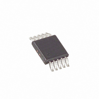
IC POT NV TRIPLE 128POS 10-USOP
Manufacturer
Maxim Integrated Products
Datasheet
1.DS3904U-020.pdf
(11 pages)
Specifications of DS3905U-020
Taps
128
Resistance (ohms)
20K
Number Of Circuits
3
Memory Type
Non-Volatile
Interface
I²C, 2-Wire Serial
Voltage - Supply
2.7 V ~ 5.5 V
Operating Temperature
-40°C ~ 85°C
Mounting Type
Surface Mount
Package / Case
10-MSOP, Micro10™, 10-uMAX, 10-uSOP
Resistance In Ohms
20K
Lead Free Status / RoHS Status
Contains lead / RoHS non-compliant
Temperature Coefficient
-
Available stocks
Company
Part Number
Manufacturer
Quantity
Price
Part Number:
DS3905U-020+
Manufacturer:
MAXIM/美信
Quantity:
20 000
NONVOLATILE MEMORY CHARACTERISTICS
(V
Triple 128-Position Nonvolatile Digital
Variable Resistor/Switch
4
Note 1:
Note 2:
Note 3:
Note 4:
Note 5:
Note 6:
Note 7:
Note 8:
Note 9:
Note 10:
Note 11:
EEPROM Writes
CC
______________________________________________________________________
= +2.7V to +5.5V, T
All voltages are referenced to ground.
Applies to A0, SDA, SCL for the DS3904 and A0, A1, A2, SDA, SCL for the DS3905. Also applies to H0, H1,
H2 for both DS3904 and DS3905 when in the high-impedance state.
I
Absolute linearity is used to determine expected resistance. Absolute linearity is defined as the deviation
from the straight line drawn from the value of the resistance at position 00h to the value of the resistance at
position 7Fh.
Relative linearity is used to determine the change of resistance between two adjacent resistor positions.
Temperature coefficient specifies the change in resistance as a function of temperature. The temperature
coefficient varies with resistor position. Limits are guaranteed by design.
A fast-mode device can be used in a standard-mode system, but the requirement t
then be met. This is automatically the case if the device does not stretch the LOW period of the SCL signal.
If such a device does stretch the LOW period of the SCL signal, it must output the next data bit to the SDA
line t
After this period, the first clock pulse is generated.
The maximum t
signal.
C
EEPROM write begins after a stop condition occurs.
PARAMETER
STBY
B
—total capacitance of one bus line in picofarads, timing referenced to 0.9 x V
RMAX
specified with SDA = SCL = V
+ t
A
SU:DAT
= +70°C.)
HD:DAT
= 1000ns + 250ns =1250ns before the SCL line is released.
has only to be met if the device does not stretch the LOW period (t
SYMBOL
CC
and A0 = GND.
CONDITIONS
50,000
MIN
CC
SU:DAT
and 0.1 x V
TYP
LOW
> 250ns must
MAX
) of the SCL
CC
.
UNITS


