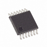
DS1845E-050+T&R Maxim Integrated Products, DS1845E-050+T&R Datasheet - Page 2

DS1845E-050+T&R
Manufacturer Part Number
DS1845E-050+T&R
Description
IC POT/MEM DUAL NV 50K 14-TSSOP
Manufacturer
Maxim Integrated Products
Datasheet
1.DS1845E-010.pdf
(14 pages)
Specifications of DS1845E-050+T&R
Taps
100, 256
Resistance (ohms)
10K, 50K
Number Of Circuits
2
Temperature Coefficient
750 ppm/°C Typical
Memory Type
Non-Volatile
Interface
I²C, 2-Wire Serial
Voltage - Supply
2.7 V ~ 5.5 V
Operating Temperature
-40°C ~ 85°C
Mounting Type
Surface Mount
Package / Case
14-TSSOP
Resistance In Ohms
10K and 50K
Lead Free Status / RoHS Status
Lead free / RoHS Compliant
PIN DESCRIPTIONS
Name TSSOP BGA
V
GND
SDA
SCL
WP
A0
A1
A2
H0
H1
L0
L1
W0
W1
NC
NC
CC
14
7
1
2
6
3
4
5
13
11
8
10
9
12
A3
D1
B2
A2
C1
A1
B1
C2
A4
B3
D3
C4
D4
B4
C3
D2
Description
Power Supply Terminal. The DS1845 will support supply
voltages ranging from +2.7V to +5.5V.
Ground Terminal.
2-Wire serial data interface. The serial data pin is for serial data
transfer to and from the DS1845. The pin is open drain and may
be wire-ORed with other open drain or open collector interfaces.
2-Wire Serial Clock Input. The serial clock input is used to
clock data into the DS1845 on rising edges and clock data out on
falling edges.
Write Protect Input. If set to logic 0, the data in memory and the
potentiometer wiper setting may be changed. If set to logic 1, both
the memory and the potentiometer wiper settings will be write
protected. The WP pin is pulled high internally.
Address Input. Pins A0, A1, and A2 are used to specify the
address of each DS1845 when used in a multi-dropped
configuration. Up to eight DS1845s may be addressed on a single
2-wire bus.
Address Input.
Address Input.
High terminal of Potentiometer 0. For both potentiometers, it is
not required that the high terminal be connected to a potential
greater than the low terminal. Voltage applied to the high terminal
of each potentiometer cannot exceed V
High terminal of Potentiometer 1.
Low terminal of Potentiometer 0. For both potentiometers, it is
not required that the low terminal be connected to a potential less
than the high terminal. Voltage applied to the low terminal of each
potentiometer cannot exceed V
Low terminal of Potentiometer 1.
Wiper terminal of Pot 0. The wiper position of Potentiometer 0
is determined by the byte at EEPROM memory location F9h.
Voltage applied to the wiper terminal of each potentiometer cannot
exceed the power supply voltage, V
Wiper terminal of Pot 1. The wiper position of Potentiometer 1
is determined by the byte at EEPROM memory location F8h.
No Connect.
No Connect.
2 of 14
CC
or go below ground.
CC
, or go below ground.
CC
or go below ground.


