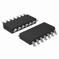
CAT521WI-T3 ON Semiconductor, CAT521WI-T3 Datasheet

CAT521WI-T3
Specifications of CAT521WI-T3
Related parts for CAT521WI-T3
CAT521WI-T3 Summary of contents
Page 1
Configured Digitally Programmable Potentiometer (DPP™): Programmable Voltage Applications FEATURES 8-bit DPP configured as a programmable voltage source in DAC-like applications Buffered wiper output Non-volatile NVRAM memory wiper storage Output voltage range includes both supply rails 1 LSB accuracy, high resolution ...
Page 2
CAT521 FUNCTIONAL DIAGRAM 3 RDY/BSY 7 PROGRAM PROG CONTROL SERIAL CLK CONTROL 4 CS CAT521 8 GND Doc. No. MD-2003 Rev. I Not Recommended for New Design 24kΩ 24kΩ 24kΩ 24kΩ SERIAL DATA OUTPUT ...
Page 3
Not Recommended for New Design ABSOLUTE MAXIMUM RATINGS Parameters Ratings Supply Voltage GND -0 Inputs CLK to GND -0 GND -0 GND -0 ...
Page 4
CAT521 POTENTIOMETER CHARACTERISTICS V = +2.7V to +5.5V REFH DD Symbol Parameter R Potentiometer Resistance POT R to RPOT Match POT Pot Resistance Tolerance Voltage on V pin REFH Voltage on V pin REFL Resolution INL ...
Page 5
Not Recommended for New Design A.C. TIMING DIAGRAM t o CLK t CSS CS t DIS PROG RDY/BSY t o © 2008 SCILLC. All rights reserved. Characteristics subject to change without notice ...
Page 6
CAT521 PIN DESCRIPTION Pin Name Function 1 V Power supply positive DD 2 CLK Clock input pin ¯¯¯¯ 3 RDY/BSY Ready/Busy output 4 CS Chip select 5 DI Serial data input pin 6 DO Serial data output pin EEPROM Programming ...
Page 7
Not Recommended for New Design No clock is necessary upon system power-up. The CAT521 internal power-on reset circuitry loads data from non-volatile memory to the DPP without using the external clock. As data transfers are edge triggered clean clock transitions ...
Page 8
CAT521 READING DATA Each time data is transferred into the DPP wiper control register currently held data is shifted out via the D0 pin, thus in every data transaction a read cycle occurs. Note, however, that the reading process is ...
Page 9
Not Recommended for New Design APPLICATION CIRCUITS + DPP CONTROL CAT521 & DATA V GND REFL V OUT For OUT + REFH CONTROL CAT521 & DATA ...
Page 10
CAT521 PACKAGE OUTLINE DRAWINGS (1)(2) PDIP 14-Lead (L) D TOP VIEW e b1 SIDE VIEW Notes: (1) All dimensions are in millimeters. Angles in degrees. (2) Complies with JEDEC MS-001. Doc. No. MD-2003 Rev. I Not Recommended for New Design ...
Page 11
Not Recommended for New Design (1)(2) SOIC 14-Lead (W) PIN#1 IDENTIFICATION TOP VIEW SIDE VIEW Notes: (1) All dimensions are in millimeters. Angles in degrees. (2) Complies with JEDEC MS-012. © 2008 SCILLC. All rights reserved. ...
Page 12
... Product Number 521 Notes: (1) All packages are RoHS compliant (Lead-free, Halogen-free). (2) Standard lead finish is Matte-Tin. (3) The device used in the above example is a CAT521WI-T2 (SOIC, Industrial Temperature, Tape & Reel). ORDERING INFORMATION CAT521WI CAT521LI Doc. No. MD-2003 Rev. I Not Recommended for New Design ...
Page 13
... Add “Not Recommended for New Design” to the top of all pages 21-Nov-08 I Change logo and fine print to ON Semiconductor ON Semiconductor and are registered trademarks of Semiconductor Components Industries, LLC (SCILLC). SCILLC reserves the right to make changes without further notice to any products herein. SCILLC makes no warranty, representation or guarantee regarding the suitability of its products for any particular purpose, nor does SCILLC assume any liability arising out of the application or use of any product or circuit, and specifically disclaims any and all liability, including without limitation special, consequential or incidental damages. “ ...


