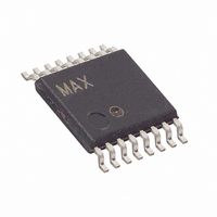
DS1856E-020+ Maxim Integrated Products, DS1856E-020+ Datasheet - Page 13

DS1856E-020+
Manufacturer Part Number
DS1856E-020+
Description
IC RES TEMP-CNTRL 20/20K 16TSSOP
Manufacturer
Maxim Integrated Products
Datasheet
1.DS1856B-050.pdf
(31 pages)
Specifications of DS1856E-020+
Taps
256
Resistance (ohms)
20K
Number Of Circuits
2
Temperature Coefficient
50 ppm/°C Typical
Memory Type
Non-Volatile
Interface
I²C, 2-Wire Serial
Voltage - Supply
2.85 V ~ 5.5 V
Operating Temperature
-40°C ~ 95°C
Mounting Type
Surface Mount
Package / Case
16-TSSOP
Resistance In Ohms
20K
Lead Free Status / RoHS Status
Lead free / RoHS Compliant
The DS1856 2-wire interface uses 8-bit addressing,
which allows up to 256 bytes to be addressed tradi-
tionally on a given 2-wire slave address. However,
since the Main Device contains more than 256 bytes, a
table scheme is used. The lower 128 bytes of the Main
Device, memory locations 00h to 7Fh, function as
expected and are independent of the currently select-
ed table. Byte 7Fh is the Table Select byte. This byte
determines which memory table will be accessed by
the 2-wire interface when address locations 80h to FFh
are accessed. Memory locations 80h to FFh are acces-
sible only through the Main Device address. The
Auxiliary Device address has no access to the tables,
but the Auxiliary Device memory can be mapped into
the Main Device’s memory space (by setting ADEN =
1). Valid values for the Table Select byte are shown in
the table below.
Table 6. Table Select Byte
Before attempting to read and write any of the bits or
bytes mentioned in this section, it is important to look at
the memory map provided in a subsequent section to
verify what level of password is required. Password
protection is described in the following section.
The DS1856 uses two 4-byte passwords to achieve
three levels of access to various memory locations. The
three levels of access are:
User Access: This is the default state after power-up. It
allows read access to standard monitoring and status
functions.
Level 1 Access: This allows access to customer data
table (Tables 00 and 01) in addition to everything grant-
ed by User access. This level is granted by entering
Password 1 (PW1).
Level 2 Access: This allows access to all memory, set-
tings, and features, in addition to everything granted by
Level 1 and User access. This level is granted by enter-
ing Password 2 (PW2).
To obtain a particular level of access, the correspond-
ing password must be entered in the Password Entry
nally Calibrated Monitors and Password Protection
Dual, Temperature-Controlled Resistors with Inter-
TABLE SELECT
BYTE
00
01
02
03
04
05
Auxiliary Device Memory
(When ADEN = 1)
Does Not Exist
Configuration
Resistor 0 Look-up Table
Resistor 1 Look-up Table
Password Protection
TABLE NAME
____________________________________________________________________
(PWE) bytes located in the Main Device at 7Bh to 7Eh.
The value entered is compared to both the PW1 and
PW2 settings located in Table 03, bytes B0h to B3h and
Table 03, bytes B4h to B7h, respectively, to determine
if access should be granted. Access is granted until
the password is changed or until power is cycled.
Writing PWE can be done with any level of access,
although PWE can never be read.
Writing PW1 and PW2 requires PW2 access. However,
PW1 and PW2 can never be read, even with PW2 access.
On power-up, PWE is set to all 1s (FFFFh). As long as
neither of the passwords are ever changed to FFFFh,
then User access is the power-up default. Likewise,
password protection can be intentionally disabled by
setting the PW2 password to FFFFh.
The following table is the legend used in the memory
map to indicate the access level required for read and
write access.
Each table in the following memory map begins with a
higher level view of a particular portion of the memory
showing information such as row (8 bytes) and byte
names. The tables are then followed, where applicable,
by an Expanded Bytes table, which shows bit names
and values. Furthermore, both tables use the permis-
sion legend to indicate the access required on a row,
byte, and bit level.
The memory map is followed by a Register Description
section, which describes bytes and bits in further detail.
Table 7. Password Permission
PERMISSION
<10>
<11>
<0>
<1>
<2>
<3>
<4>
<5>
<6>
<7>
<8>
<9>
At least one byte in the row is different than
the rest of the row, so look at each byte
separately for permissions.
READ
PW2
PW1
PW2
PW2
NA
NA
all
all
all
all
all
all (The part also writes to
PW2 + mode_bit
Memory Map
this byte.)
WRITE
PW2
PW1
PW2
PW2
PW1
NA
NA
all
all
13


