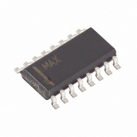
DS1808Z-050+T&R Maxim Integrated Products, DS1808Z-050+T&R Datasheet - Page 6

DS1808Z-050+T&R
Manufacturer Part Number
DS1808Z-050+T&R
Description
IC POT DUAL LOG HV 50K 16-SOIC
Manufacturer
Maxim Integrated Products
Datasheet
1.DS1808Z-050.pdf
(17 pages)
Specifications of DS1808Z-050+T&R
Taps
32
Resistance (ohms)
45K
Number Of Circuits
2
Temperature Coefficient
750 ppm/°C Typical
Memory Type
Volatile
Interface
I²C, 2-Wire Serial
Voltage - Supply
4.5 V ~ 5.5 V, ±4.5 V ~ 13.2 V
Operating Temperature
-40°C ~ 85°C
Mounting Type
Surface Mount
Package / Case
16-SOIC (3.9mm Width)
Resistance In Ohms
45K
Lead Free Status / RoHS Status
Lead free / RoHS Compliant
The master device generates all serial clock pulses and the start and stop conditions. A transfer is ended
with a stop condition or with a repeated start condition. Since a repeated start condition is also the
beginning of the next serial transfer, the bus will not be released.
The DS1808 may operate in the following two modes:
1. Slave receiver mode: Serial data and clock are received through SDA and SCL respectively. After
2. Slave transmitter mode: The first byte is received and handled as in the slave receiver mode.
3. Slave Address: command/control byte is the first byte received following the start condition from the
Following the START condition, the DS1808 monitors the SDA bus checking the device type identifier
being transmitted. Upon receiving the 0101 control code, the appropriate device address bits, and the
read/write bit, the slave device outputs an acknowledge signal on the SDA line.
COMMAND AND PROTOCOL
The command and protocol structure of the DS1808 allows the user to read from or write to the
potentiometer(s). Additionally, the 2-wire command/protocol structure of the DS1808 will support eight
different devices and a maximum of 16 channels that can be uniquely controlled. The command
structures for the device are presented in Figures 3, 4, 5, and 6. Potentiometer data values and
command/control values are always transmitted most significant bit (MSB) first. During communications,
the receiving unit always generates the acknowledgement.
each byte is received, an acknowledge bit is transmitted. Start and stop conditions are recognized as
the beginning and end of a serial transfer. Address recognition is performed by hardware after
reception of the slave (device) address and direction bit.
However, in this mode the direction bit will indicate that the transfer direction is reversed. Serial data
is transmitted on SDA by the DS1808 while the serial clock is input on SCL. Start and stop conditions
are recognized as the beginning and end of a serial transfer.
master device. The command/control byte consists of a 4-bit control code. For the DS1808, this is set
as 0101 binary for read/write operations. The next three bits of the command/control byte are the
device select bits or slave address (A2, A1, A0). They are used by the master device to select which
of eight devices is to be accessed. When reading or writing the DS1808, the device select bits must
match the device select pins (A2, A1, A0). The last bit of the command/control byte (R/W) defines
the operation to be performed. When set to a 1, a read operation is selected, and when set to a 0, a
write operation is selected.
6 of 17


