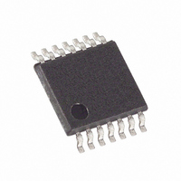
MAX5437EUD+T Maxim Integrated Products, MAX5437EUD+T Datasheet - Page 7

MAX5437EUD+T
Manufacturer Part Number
MAX5437EUD+T
Description
IC POT DGTL 128-TAP 15V 14-TSSOP
Manufacturer
Maxim Integrated Products
Datasheet
1.MAX5436EUBT.pdf
(11 pages)
Specifications of MAX5437EUD+T
Taps
128
Resistance (ohms)
50K
Number Of Circuits
1
Temperature Coefficient
35 ppm/°C Typical
Memory Type
Volatile
Interface
SPI, 3-Wire Serial
Voltage - Supply
10 V ~ 30 V, ±5 V ~ 15 V
Operating Temperature
-40°C ~ 85°C
Mounting Type
Surface Mount
Package / Case
14-TSSOP
Resistance In Ohms
50K
Lead Free Status / RoHS Status
Lead free / RoHS Compliant
The MAX5436–MAX5439 use a 3-wire SPI/QSPI/
MICROWIRE-compatible serial data interface to control
the wiper position. This write-only interface contains
three inputs: chip select (CS), data in (DIN), and serial
clock (SCLK). When CS is taken low, data from DIN is
synchronously loaded into the serial shift register on the
rising edge of each SCLK pulse (Figure 2). The 8-bit
data word requires 8 clock pulses to input the serial
data. Note that the first bit of the data word, D7, is
unused and should be ignored. Therefore, the second
rising edge of SCLK loads the MSB. After all the data
bits have been shifted in, they are latched into the
potentiometer control register when CS transitions from
low to high, the wiper position is then updated. Note
that if CS is not kept low during the entire data stream,
the data will be corrupted and the device will need to
be reloaded.
The MAX5436–MAX5439 have been designed so that
any of the supplies can turn on first without causing any
unwanted crowbar currents to flow. Note that both digital
and analog supplies are required to power up the wiper
and uncommitted amplifier (MAX5437/MAX5439 only).
±15V, 128-Tap, Low-Drift Digital Potentiometers
MAX5436/
MAX5438
10
—
—
—
—
1
2
3
4
5
6
7
8
9
PIN
Applications Information
MAX5437/
MAX5439
_______________________________________________________________________________________
10
11
12
13
14
1
2
3
4
5
6
7
8
9
Digital Interface Operation
Detailed Description
Power-Up Sequencing
NAME
SHDN
SCLK
GND
OUT
V
V
DIN
V
IN+
CS
IN-
W
DD
H
CC
L
SS
Serial Clock Input
Serial Data Input
Chip Select
Amplifier Shutdown
Analog and Digital Ground
Negative Analog Supply. Bypass with a 0.1µF capacitor to GND.
Amplifier Output
Amplifier Negative Input
Amplifier Positive Input
Positive Analog Supply. Bypass with a 0.1µF capacitor to GND.
High Terminal of Resistor
Wiper Terminal of Resistor
Low Terminal of Resistor
Digital Supply. Bypass with a 0.1µF capacitor to GND.
The MAX5436/MAX5438 are used with the MAX427 to
make a digitally adjustable gain circuit as shown in
Figure 4. The normal feedback resistor is replaced with
the MAX5436/MAX5438 in a variable-resistor configura-
tion so that the gain of the circuit can be digitally con-
trolled. The MAX5437/MAX5439 can use the internal
high-voltage amplifier to make this digitally adjustable
gain circuit.
The MAX5436–MAX5439 are ideal for LCDs that require
separate voltage for contrast control in addition to the
main supply voltage. Figure 5a shows the MAX5436–
MAX5439 being used for LCD contrast control along with
the MAX629, which provides the LCD supply voltage. A
similar circuit with an additional buffer circuit is shown in
Figure 5b.
DESCRIPTION
LCD Biasing Control Applications
Adjustable Gain Amplifier
Pin Description
7


