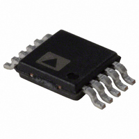
AD5201BRM10 Analog Devices Inc, AD5201BRM10 Datasheet - Page 12

AD5201BRM10
Manufacturer Part Number
AD5201BRM10
Description
IC DGTL POT 10K 33POS 10-MSOP
Manufacturer
Analog Devices Inc
Datasheet
1.AD5200BRMZ10.pdf
(16 pages)
Specifications of AD5201BRM10
Rohs Status
RoHS non-compliant
Taps
33
Resistance (ohms)
10K
Number Of Circuits
1
Temperature Coefficient
500 ppm/°C Typical
Memory Type
Volatile
Interface
SPI, 3-Wire Serial
Voltage - Supply
2.7 V ~ 5.5 V, ±2.3 V ~ 2.7 V
Operating Temperature
-40°C ~ 85°C
Mounting Type
Surface Mount
Package / Case
10-MSOP, Micro10™, 10-uMAX, 10-uSOP
Resistance In Ohms
10K
AD5200/AD5201
The general equation determining the digitally programmed
output resistance between W and B is:
where:
D
R
R
R
R
AB
W
WB
WB
is the decimal equivalent of the data contained in
RDAC latch.
is the nominal end-to-end resistance.
is the wiper resistance contributed by the on-resistance
of the internal switch.
( )
( )
D
D
=
=
255
D5
D4
D3
D2
D1
D0
32
D
DECODER
D7
D6
D5
D4
D3
D2
D1
D0
DECODER
LATCH &
D
LATCH &
RDAC
RDAC
R
SHDN
R
SHDN
AB
AB
+
+
50 Ω
R
R
R
R
50 Ω
R
R
R
A
B
A
B
SW
SW
SW
SW
SW
SW
SW
DIGITAL CIRCUITRY
OMITTED FOR CLARITY
DIGITAL CIRCUITRY
OMITTED FOR CLARITY
SW
SW
SW
SW
2
2
SHDN
2
2
2
SHDN
N
N
1
0
N
N
N
1
0
for AD5201
for AD5200
1
2
1
2
R
R
W
W
2
R
R
2
N
AB
AB
N
–1
(1)
(2)
Note D in AD5200 is between 0 to 255 for 256 positions. On
the other hand, D in AD5201 is between 0 to 32 so that 33
positions can be achieved due to the slight internal structure
difference, Figure 2b.
Again if R
W, the following output resistance between W to B will be set
for the following RDAC latch codes:
D
(DEC)
255
128
1
0
D
(DEC)
32
16
1
0
Note that in the zero-scale condition a finite wiper resistance of
50 Ω is present. Care should be taken to limit the current flow
between W and B in this state to no more than ± 20 mA to avoid
degradation or possible destruction of the internal switch contact.
Like the mechanical potentiometer the RDAC replaces, it is
totally symmetrical. The resistance between the wiper W and
Terminal A also produces a digitally controlled resistance R
When these terminals are used, the B terminal should be tied to
the wiper. Setting the resistance value for R
mum value of resistance and decreases as the data loaded in
the latch is increased in value. The general equation for this
operation is:
Similarly, D in AD5200 is between 0 to 255, whereas D in
AD5201 is between 0 to 32.
For R
W, the following output resistance between W and A will be set
for the following RDAC latch codes:
R
R
WA
WA
AB
( )
( )
= 10 kΩ and B terminal is opened or tied to the wiper
D
D
AB
R
( )
10050
5070
89
50
R
( )
10050
5050
363
50
=
=
= 10 kΩ and A terminal can be opened or tied to
WB
WB
(
(
255
32
AD5200 Wiper-to-B Resistance
AD5201 Wiper-to-B Resistance
255
32
−
−
D
D
)
)
R
R
AB
Full-Scale (R
Full-Scale (R
1 LSB
Output State
Midscale
1 LSB
Zero-Scale (Wiper Contact Resistance)
Output State
Midscale
Zero-Scale (Wiper Contact Resistance)
AB
+
+
50 Ω
50 Ω
AB
AB
+ R
+ R
WA
for AD5200
for AD5201
W
W
)
)
starts at a maxi-
WA
(3)
(4)
.


