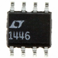
LTC1446CS8#PBF Linear Technology, LTC1446CS8#PBF Datasheet - Page 5

LTC1446CS8#PBF
Manufacturer Part Number
LTC1446CS8#PBF
Description
IC D/A CONV 12BIT R-R DUAL 8SOIC
Manufacturer
Linear Technology
Datasheet
1.LTC1446CN8PBF.pdf
(12 pages)
Specifications of LTC1446CS8#PBF
Settling Time
14µs
Number Of Bits
12
Data Interface
Serial
Number Of Converters
2
Voltage Supply Source
Single Supply
Power Dissipation (max)
5mW
Operating Temperature
0°C ~ 70°C
Mounting Type
Surface Mount
Package / Case
8-SOIC (3.9mm Width)
Number Of Channels
2
Resolution
12b
Interface Type
Serial (3-Wire)
Single Supply Voltage (typ)
5V
Dual Supply Voltage (typ)
Not RequiredV
Power Supply Requirement
Single
Output Type
Voltage
Integral Nonlinearity Error
5LSB
Single Supply Voltage (min)
4.5V
Single Supply Voltage (max)
5.5V
Dual Supply Voltage (min)
Not RequiredV
Dual Supply Voltage (max)
Not RequiredV
Operating Temp Range
0C to 70C
Operating Temperature Classification
Commercial
Mounting
Surface Mount
Pin Count
8
Package Type
SOIC N
Lead Free Status / RoHS Status
Lead free / RoHS Compliant
Available stocks
Company
Part Number
Manufacturer
Quantity
Price
TYPICAL PERFORMANCE CHARACTERISTICS
CLK: The Serial Interface Clock.
D
CS/LD: The Serial Interface Enable and Load Control.
When CS/LD is low the CLK signal is enabled, so the data
can be clocked in. When CS/LD is pulled high data is
loaded from the shift register into the DAC registers,
updating the DAC outputs.
PIN
IN
1.2
1.1
1.0
0.9
0.8
0.7
0.6
0.5
U
: The Serial Interface Data.
0.5
LTC1446L Supply Current vs Logic
Input Voltage
FUNCTIONS
1.0
U
LOGIC INPUT VOLTAGE (V)
1.5
U
2.0
W
2.5
1446/46L G10
U
3.0
(2V/DIV)
(5V/DIV)
CS/LD
V
970
960
950
940
930
920
910
900
OUT
–55 –35 –15
LTC1446 Supply Current vs
Temperature
Large Signal Transient Response
TEMPERATURE ( C)
TIME (10 s/DIV)
5
25
V
V
V
CC
CC
D
on the rising edge of the serial clock.
GND: Ground.
V
V
4.5V V
(LTC1446L). Requires a 0.1 F bypass capacitor to
ground.
CC
45
OUT A
CC
OUT
= 5.5V
= 5V
= 4.5V
: Positive Supply Input.
65
: The output of the shift register which becomes valid
,V
85 105
1446/46L G11
CC
OUT B
1446L G13
125
5.5V (LTC1446), 2.7V V
: Buffered DAC Outputs.
700
690
680
670
660
650
640
630
620
LTC1446/LTC1446L
– 55
LTC1446L Supply Current
vs Temperature
– 35
V
V
–15
V
CC
CC
CC
= 3.3V
= 2.7V
= 3V
TEMPERATURE ( C)
5
25
CC
45
65
5.5V
85
1446/46L G12
105
5
125


