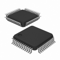
LTC2757BILX#PBF Linear Technology, LTC2757BILX#PBF Datasheet - Page 9

LTC2757BILX#PBF
Manufacturer Part Number
LTC2757BILX#PBF
Description
IC DAC 18BIT PAR 48LQFP
Manufacturer
Linear Technology
Series
SoftSpan™r
Datasheet
1.LTC2757BILXPBF.pdf
(20 pages)
Specifications of LTC2757BILX#PBF
Settling Time
2.1µs
Number Of Bits
18
Data Interface
Parallel
Number Of Converters
1
Voltage Supply Source
Single Supply
Operating Temperature
-40°C ~ 85°C
Mounting Type
Surface Mount
Package / Case
48-LQFP
Lead Free Status / RoHS Status
Lead free / RoHS Compliant
Power Dissipation (max)
-
Available stocks
Company
Part Number
Manufacturer
Quantity
Price
V
pin can be used to null unipolar offset or bipolar zero error.
The offset change expressed in LSB is the same for any
output range. See System Offset and Gain Adjustments in
the Operation section. Tie to ground if not used.
I
negative input (summing junction) of the I/V converter
amplifi er.
R
to the output of the I/V converter amplifi er. The DAC output
current from I
the R
R
provide the translation of the output voltage range for
bipolar spans. Accepts up to ±15V; normally tied to the
positive reference voltage. These pins are internally shorted
together.
BLOCK DIAGRAM
PIN FUNCTIONS
OUT1
OSADJ
FB
OFS
(Pins 41, 42): DAC Feedback Resistor. Normally tied
FB
(Pins 43, 44): Bipolar Offset Network. These pins
(Pin 40): DAC current output; normally tied to the
(Pin 39): DAC Offset Adjust Pin. This voltage-control
pins. These pins are internally shorted together.
OUT1
fl ows through the feedback resistor to
36
35
34
33
20
21
R
1, 2
WR
UPD
READ
D/S
CLR
M-SPAN
IN
48
20k
R1
2.56M
GE
ADJ
CONTROL
LOGIC
47
R
COM
20k
R2
3, 37, 38
REF
45, 46
REGISTER
REGISTER
SPAN I/O
18-BIT DAC WITH SPAN SELECT
S2-S0
INPUT
PORT
3
3
3
DAC
I/O
REF (Pins 45, 46): Feedback Resistor for the Reference
Inverting Amplifi er, and Reference Input for the DAC.
Normally tied to the output of the reference inverting
amplifi er. Typically –5V; accepts up to ±15V. These pins
are internally shorted together.
R
tied to the negative input of the external reference invert-
ing amplifi er.
GE
pin can be used to null gain error or to compensate for
reference errors. The gain error change expressed in LSB
is the same for any output range. See System Offset and
Gain Adjustments in the Operation section. Tie to ground
if not used.
COM
8-16, 23-31
ADJ
R
43, 44
OFS
(Pin 47): Center Tap Point of R
(Pin 48): Gain Adjust Pin. This voltage-control
REGISTER
REGISTER
DATA I/O
D17-D0
18
18
18
INPUT
PORT
DAC
I/O
R
41, 42
FB
V
I
I
OSADJ
OUT2S
OUT2F
I
OUT1
2757 BD
39
40
6
5
IN
and REF . Normally
LTC2757
9
2757f


