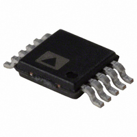
AD5624RBRMZ-5 Analog Devices Inc, AD5624RBRMZ-5 Datasheet - Page 23

AD5624RBRMZ-5
Manufacturer Part Number
AD5624RBRMZ-5
Description
IC DAC NANO 12BIT 2.5V 10-MSOP
Manufacturer
Analog Devices Inc
Series
nanoDAC™r
Specifications of AD5624RBRMZ-5
Data Interface
DSP, MICROWIRE™, QSPI™, Serial, SPI™
Settling Time
3µs
Number Of Bits
12
Number Of Converters
4
Voltage Supply Source
Single Supply
Operating Temperature
-40°C ~ 105°C
Mounting Type
Surface Mount
Package / Case
10-MSOP, Micro10™, 10-uMAX, 10-uSOP
Resolution (bits)
12bit
Sampling Rate
287kSPS
Input Channel Type
Serial
Supply Voltage Range - Analog
2.7V To 3.6V, 4.5V To 5.5V
Supply Current
950µA
Number Of Channels
4
Resolution
12b
Conversion Rate
287KSPS
Interface Type
Serial (3-Wire, SPI, QSPI, Microwire)
Single Supply Voltage (typ)
5V
Dual Supply Voltage (typ)
Not RequiredV
Architecture
Resistor-String
Power Supply Requirement
Single
Output Type
Voltage
Integral Nonlinearity Error
±1LSB
Single Supply Voltage (min)
4.5V
Single Supply Voltage (max)
5.5V
Dual Supply Voltage (min)
Not RequiredV
Dual Supply Voltage (max)
Not RequiredV
Operating Temp Range
-40C to 105C
Operating Temperature Classification
Industrial
Mounting
Surface Mount
Pin Count
10
Package Type
MSOP
Lead Free Status / RoHS Status
Lead free / RoHS Compliant
Power Dissipation (max)
-
Lead Free Status / Rohs Status
Compliant
Available stocks
Company
Part Number
Manufacturer
Quantity
Price
Part Number:
AD5624RBRMZ-5
Manufacturer:
ADI/亚德诺
Quantity:
20 000
LDAC FUNCTION
The AD5624R/AD5644R/AD5664R DACs have double-
buffered interfaces consisting of two banks of registers: input
registers and DAC registers. The input registers are connected
directly to the input shift register and the digital code is tra
ferred to the relevant input register on completion of a valid
write sequence. The DAC registers contain the digital code u
by the resistor strings.
The double-buffered int
simultaneous updating of all DAC outputs. The user can write
to three of the input registers individually and then write to t
remaining input register, updating all DAC registers simulta-
neously. Command 010 is reserved for this software LDAC.
Access to the DAC registers is
The LDAC register contains two modes of operation for ea
DAC channel. The DAC channels are selected by setting th
bits of the 4-bit LDAC register (DB3, DB2, DB1, a
Command 110 is reserved for setting up the LDAC register.
When the LDAC bit register is set lo
registers are latched and the input register
without affecting the contents of the DAC r
LDAC
be
tra
This is equivalent to
nently low for the se
u
o
d
Table 16. 24-Bit Input Shift Register Contents for LDAC Setu
DB23 to DB22
(MSB)
x
Don’t care
Table 17. 24-Bit Input Shift Register Contents for Internal Re
DB23 to DB22
(M
x
Don’t care
pdate mode. See Table 1
peration. See Table 16 fo
uring the LDAC register
com
nsferred to them on th
SB)
e transparent and t
bit register is set hi
DB21
1
lected
havin
DB21
1
erface is useful if the user requires
Command bits
Command bits (C2 to C0)
e falling edge of the 24
4 for the LDAC
he contents of
gh, however, the DAC
r contents of the input s
setup command.
g an LDAC hardware pin tied perma-
DAC channel, that
(C2 to C0)
DB20
1
controlled by the LDAC function.
DB20
1
w, the corresponding DAC
DB19
0
the inp
regi
s can change state
egisters. When the
DB19
1
ster mode of
is, synchronous
ut registers are
th
DB18
x
registers
hift register
nd DB0).
SCLK pulse.
(A2 to A0); don
Address b
DB18
x
DB17
x
ch
ns-
e
Address bits (A2 to A0)
Rev. B | Page 23 of 28
sed
he
p Command for the AD5624R/AD5644R/AD5664R
ference Setup Command
its
’t care
DB17
x
DB16
x
This flexibility is useful in applications where the user wants to
update select channels simultaneously, while the rest of the
channels update synchronously.
Table 14. LDAC Register Mode of Operation
LDAC Bits
(DB3 to DB0)
0
1
INTERN L REF
Th
can be turned on or off by setting a software programmable bit,
DB0, in the control register. Table 15 shows how the state of the
bit corresponds to the mode of operation. Command 111 is
reserved for setting up the internal reference (see Table 8).
Table 16 shows how the state of the bits in the input shift
register corresponds to the mode of operation of the device
during internal reference setup.
Table 15. Reference Setup Register
Internal Reference
Setup Register
(DB0)
0
1
e on-chi eferen
DB15 to DB4
x
Don’t care
DB16
x
A
p r
DB15 to DB1
x
Don’t care
AD5624R/AD5644R/AD5664R
ERENCE SETUP
ce is off at power-up by default. This
DB3
DAC D
LDAC Mode of O
Normal operation (default), DAC register
update is controlled by write command.
The DAC registers are updated after new
data is read in on the falling edge of the
24
Action
Reference off (default)
Reference on
Set bit to 0 or 1 for required mode of
th
operation on respective channel
SCLK puls
DB2
DAC C
DB0 (LSB)
1/0
Reference setup register
e.
peration
DB1
DAC B
DB0 (LSB)
DAC A
reference


