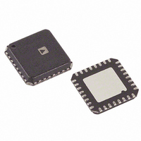
AD9707BCPZ Analog Devices Inc, AD9707BCPZ Datasheet - Page 36

AD9707BCPZ
Manufacturer Part Number
AD9707BCPZ
Description
IC DAC TX 14BIT 175MSPS 32-LFCSP
Manufacturer
Analog Devices Inc
Series
TxDAC®r
Datasheet
1.AD9704BCPZ.pdf
(52 pages)
Specifications of AD9707BCPZ
Data Interface
Serial
Settling Time
11ns
Number Of Bits
14
Number Of Converters
1
Voltage Supply Source
Analog and Digital
Power Dissipation (max)
50mW
Operating Temperature
-40°C ~ 85°C
Mounting Type
Surface Mount
Package / Case
32-LFCSP
Resolution (bits)
14bit
Sampling Rate
175MSPS
Input Channel Type
Parallel
Supply Voltage Range - Analogue
1.7V To 3.6V
Supply Voltage Range - Digital
1.7V To 3.6V
Supply
RoHS Compliant
Lead Free Status / RoHS Status
Lead free / RoHS Compliant
For Use With
AD9707-EBZ - BOARD EVAL FOR AD9707
Lead Free Status / RoHS Status
Lead free / RoHS Compliant
Available stocks
Company
Part Number
Manufacturer
Quantity
Price
Company:
Part Number:
AD9707BCPZ
Manufacturer:
ADI
Quantity:
1 134
Company:
Part Number:
AD9707BCPZ
Manufacturer:
ADI
Quantity:
208
Part Number:
AD9707BCPZ
Manufacturer:
ADI
Quantity:
20 000
Company:
Part Number:
AD9707BCPZRL7
Manufacturer:
DIALIGHT
Quantity:
4 000
AD9704/AD9705/AD9706/AD9707
The digital interface is implemented using an edge-triggered
master/slave latch. The DAC output updates on the rising edge
of the clock and is designed to support a clock rate as high as
175 MSPS. The clock can be operated at any duty cycle that meets
the specified latch pulse width. The setup and hold times can
also be varied within the clock cycle, as long as the specified
minimum times are met, although the location of these transition
edges may affect digital feedthrough and distortion performance.
Best performance is typically achieved when the input data
transitions on the falling edge of a 50% duty cycle clock.
CLOCK INPUT
A configurable clock input allows the device to be operated in
a single-ended or a differential clock mode. The mode selection
can be controlled either by the CMODE pin, if the device is in pin
mode; or through SPI Register 0x02, Bit 2 (CLKDIFF), if the SPI
is enabled. Connecting CMODE to CLKCOM selects the single-
ended clock input. In this mode, the CLK+ input is driven with
rail-to-rail swings, and the CLK− input is left floating. If CMODE
is connected to CLKVDD, the differential receiver mode is selected.
In this mode, both inputs are high impedance. Table 25 gives a
summary of clock mode control. There is no significant perform-
ance difference between the clock input modes.
Table 25. Clock Mode Selection
SPI Disabled
CMODE Pin
CLKCOM
CLKVDD
In differential input mode, the clock input functions as a high
impedance differential pair. The common-mode level of the
CLK+ and CLK− inputs can vary from 0.75 V to 2.25 V, and the
differential voltage can be as low as 0.5 V p-p. This mode can be
used to drive the clock with a differential sine wave because the
high gain bandwidth of the differential inputs converts the sine
wave into a single-ended square wave internally.
DIGITAL
SPI Enabled
Register 0x02, Bit 2
0
1
INPUT
Figure 79. Equivalent Digital Input
DVDD
Single-ended
Differential
Clock Input Mode
Rev. A | Page 36 of 52
DAC TIMING
Input Clock and Data Timing Relationship
Dynamic performance in a DAC is dependent on the relation-
ship between the position of the clock edges and the time at
which the input data changes. The AD9704/AD9705/AD9706/
AD9707 are rising-edge triggered and so exhibits dynamic
performance sensitivity when the data transition is close to
this edge. In general, the goal when applying the AD9704/
AD9705/AD9706/AD9707 is to make the data transition close
to the falling clock edge. This becomes more important as the
sample rate increases. Figure 80 shows the relationship of SFDR
to clock placement with different sample rates.
POWER DISSIPATION
The power dissipation, P
AD9707 is dependent on several factors that include
•
•
•
•
Power dissipation is directly proportional to the analog supply
current, I
to a fixed current plus I
proportional to f
output frequencies. Figure 83 shows I
scale sine wave output ratios (f
with DVDD = 3.3 V. I
and is higher for differential clock operation than for single-
ended operation, as shown in Figure 85. This difference in clock
current is due primarily to the differential clock receiver, which is
disabled in single-ended clock mode.
The power supply voltages (AVDD, CLKVDD, and
DVDD)
The full-scale current output, I
The update rate, f
The reconstructed digital input waveform
95
90
85
80
75
70
65
60
55
50
45
AVDD
–4
DATA EDGE WITH RESPECT TO RISING CLOCK EDGE (ns)
, and the digital supply current, I
CLOCK
Figure 80. SFDR vs. Clock Placement
–3
CLKVDD
and increases with increasing analog
CLOCK
OUTFS
D
, of the AD9704/AD9705/AD9706/
, as shown in Figure 81. I
–2
is directly proportional to f
OUT
/f
CLOCK
OUTFS
DVDD
f
f
CLOCK
–1
) for various update rates
CLOCK
as a function of full-
= 125MSPS
DVDD
= 80MSPS
. I
0
AVDD
DVDD
is equal
CLOCK
1
is


