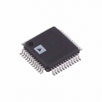
AD9765ASTZ Analog Devices Inc, AD9765ASTZ Datasheet - Page 25

AD9765ASTZ
Manufacturer Part Number
AD9765ASTZ
Description
IC DAC 12BIT DUAL 125MSPS 48LQFP
Manufacturer
Analog Devices Inc
Series
TxDAC+®r
Datasheet
1.AD9763ASTZ.pdf
(44 pages)
Specifications of AD9765ASTZ
Data Interface
Parallel
Settling Time
35ns
Number Of Bits
12
Number Of Converters
2
Voltage Supply Source
Analog and Digital
Power Dissipation (max)
450mW
Operating Temperature
-40°C ~ 85°C
Mounting Type
Surface Mount
Package / Case
48-LQFP
Resolution (bits)
12bit
Sampling Rate
125MSPS
Input Channel Type
Parallel
Supply Voltage Range - Analog
3V To 5.5V
Supply Voltage Range - Digital
2.7V To 5.5V
Lead Free Status / RoHS Status
Lead free / RoHS Compliant
For Use With
AD9765-EBZ - BOARD EVAL FOR AD9765
Lead Free Status / RoHS Status
Lead free / RoHS Compliant, Lead free / RoHS Compliant
Available stocks
Company
Part Number
Manufacturer
Quantity
Price
Company:
Part Number:
AD9765ASTZ
Manufacturer:
ADI
Quantity:
345
Company:
Part Number:
AD9765ASTZ
Manufacturer:
Analog Devices Inc
Quantity:
10 000
Part Number:
AD9765ASTZ
Manufacturer:
ADI/亚德诺
Quantity:
20 000
Company:
Part Number:
AD9765ASTZRL
Manufacturer:
Analog Devices Inc
Quantity:
10 000
Interleaved Mode Timing
When the MODE pin is at Logic 0, the AD9763/AD9765/AD9767
operate in interleaved mode (refer to Figure 61). In addition,
WRT1 functions as IQWRT, CLK1 functions as IQCLK, WRT2
functions as IQSEL, and CLK2 functions as IQRESET.
Data enters the device on the rising edge of IQWRT. The logic level
of IQSEL steers the data to either Channel Latch 1 (IQSEL = 1) or
to Channel Latch 2 (IQSEL = 0). For proper operation, IQSEL
must change state only when IQWRT and IQCLK are low.
When IQRESET is high, IQCLK is disabled. When IQRESET
goes low, the next rising edge on IQCLK updates both DAC
latches with the data present at their inputs. In the interleaved
mode, IQCLK is divided by 2 internally. Following this first
rising edge, the DAC latches are only updated on every other
rising edge of IQCLK. In this way, IQRESET can be used to
synchronize the routing of the data to the DACs.
Similar to the order of CLK and WRT in dual-port mode,
IQCLK must occur before or simultaneously with IQWRT.
Timing specifications for interleaved mode are shown in Figure 64
and Figure 66.
The digital inputs are CMOS compatible with logic thresholds,
V
(DVDDx), or
At 5 V it is permissible to drive IQWRT and IQCLK together as
shown in Figure 65, but at 3.3 V the interleaved data transfer is
not reliable.
THRESHOLD
DATA IN
V
IQWRT
IQCLK
IQSEL
THRESHOLD
, set to approximately half the digital positive supply
Figure 64. 5 V or 3.3 V Interleaved Mode Timing
= DVDDx /2(±20%)
t
H
*
500 ps
t
S
t
PD
500 ps
t
H
t
LPW
Rev. F | Page 25 of 44
The internal digital circuitry of the AD9763/AD9765/AD9767
is capable of operating at a digital supply of 3.3 V or 5 V. As a
result, the digital inputs can also accommodate TTL levels when
DVDD1/DVDD2 is set to accommodate the maximum high
level voltage (V
of 3.3 V typically ensures proper compatibility with bipolar TTL
logic families. Figure 67 shows the equivalent digital input
circuit for the data and clock inputs. The sleep mode input is
similar, with the exception that it contains an active pull-down
circuit, thus ensuring that the AD9763/AD9765/AD9767
remains enabled if this input is left disconnected.
INTERLEAVED
DAC OUTPUT
DAC OUTPUT
DATA IN
IQWRT
IQCLK
IQSEL
I
I
OUTA
OUTB
IQRESET
*APPLIES TO FALLING EDGE OF IQCLK/IQWRT AND IQSEL ONLY.
OR
PORT 1
PORT 2
IQWRT
IQCLK
IQSEL
DATA
Figure 65. 5 V Only Interleaved Mode Timing
OH(MAX)
DIGITAL
xx
t
Figure 66. Interleaved Mode Timing
Figure 67. Equivalent Digital Input
H
INPUT
*
) of the TTL drivers. A DVDD1/DVDD2
D1
xx
xx
AD9763/AD9765/AD9767
t
S
D2
t
PD
t
H
D3
t
LPW
DVDD1
D1
D2
D4
D5
D3
D4


