MAX5531ETC+ Maxim Integrated Products, MAX5531ETC+ Datasheet - Page 12
MAX5531ETC+
Manufacturer Part Number
MAX5531ETC+
Description
IC DAC 12BIT SGL ULP 12-TQFN
Manufacturer
Maxim Integrated Products
Datasheet
1.MAX5531ETC.pdf
(19 pages)
Specifications of MAX5531ETC+
Settling Time
660µs
Number Of Bits
12
Data Interface
MICROWIRE™, QSPI™, Serial, SPI™
Number Of Converters
1
Voltage Supply Source
Single Supply
Power Dissipation (max)
1.35mW
Operating Temperature
-40°C ~ 85°C
Mounting Type
Surface Mount
Package / Case
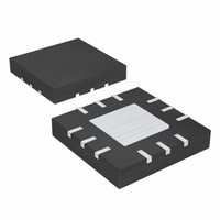
12-TQFN Exposed Pad
Number Of Dac Outputs
1
Resolution
12 bit
Interface Type
Serial (SPI)
Supply Voltage (max)
5.5 V
Supply Voltage (min)
1.8 V
Maximum Operating Temperature
+ 85 C
Mounting Style
SMD/SMT
Minimum Operating Temperature
- 40 C
Supply Current
0.007 mA
Voltage Reference
Internal
Lead Free Status / RoHS Status
Lead free / RoHS Compliant


Ultra-Low-Power, 12-Bit,
Voltage-Output DACs
The MAX5530/MAX5531 single, 12-bit, ultra-low-power,
voltage-output DACs offer Rail-to-Rail buffered voltage
outputs. The DACs operate from a 1.8V to 5.5V supply
and require only 6µA (max) supply current. These
devices feature a shutdown mode that reduces overall
current, including the reference input current, to just
0.18µA. The MAX5531 includes an internal reference
that saves additional board space and can source up
to 8mA, making it functional as a system reference. The
16MHz, 3-wire serial interface is compatible with SPI,
QSPI, and MICROWIRE protocols. When V
applied, all DAC outputs are driven to zero scale with
virtually no output glitch. The MAX5530/MAX5531 out-
put buffers are configured in force sense allowing users
to externally set voltage gains on the output (an output
amplifier inverting input is available). These devices
come in a 4mm x 4mm thin QFN package.
12
______________________________________________________________________________________
SCLK
DIN
CS
Detailed Description
CONTROL
CONTROL
REGISTER
POWER-
DOWN
LOGIC
SHIFT
AND
REGISTER
INPUT
PROGRAMMABLE
V
DD
DD
GND
REFERENCE
2-BIT
is
MAX5531
REGISTER
DAC
The MAX5530/MAX5531 use a 3-wire serial interface
compatible with SPI, QSPI, and MICROWIRE protocols
(Figures 1 and 2).
The MAX5530/MAX5531 include a single, 16-bit, input
shift register. Data loads into the shift register through
the serial interface. CS must remain low until all 16 bits
are clocked in. Data loads MSB first, D11–D0. The 16
bits consist of 4 control bits (C3–C0) and 12 data bits
(D11–D0) (see Table 1). The control bits C3–C0 control
the MAX5530/MAX5531, as outlined in Table 2.
Each DAC channel includes two registers: an input reg-
ister and a DAC register. The input register holds input
data. The DAC register contains the data updated to
the DAC output.
The double-buffered register configuration allows any
of the following:
• Loading the input registers without updating the DAC
• Updating the DAC registers from the input registers
• Updating all the input and DAC registers simultaneously
registers
BUF
REF
12-BIT DAC
MAX5531 Functional Diagram
REFOUT
OUT
FB
Digital Interface
Related parts for MAX5531ETC+
Image
Part Number
Description
Manufacturer
Datasheet
Request
R

Part Number:
Description:
MAX7528KCWPMaxim Integrated Products [CMOS Dual 8-Bit Buffered Multiplying DACs]
Manufacturer:
Maxim Integrated Products
Datasheet:
Part Number:
Description:
Single +5V, fully integrated, 1.25Gbps laser diode driver.
Manufacturer:
Maxim Integrated Products
Datasheet:
Part Number:
Description:
Single +5V, fully integrated, 155Mbps laser diode driver.
Manufacturer:
Maxim Integrated Products
Datasheet:
Part Number:
Description:
VRD11/VRD10, K8 Rev F 2/3/4-Phase PWM Controllers with Integrated Dual MOSFET Drivers
Manufacturer:
Maxim Integrated Products
Datasheet:
Part Number:
Description:
Highly Integrated Level 2 SMBus Battery Chargers
Manufacturer:
Maxim Integrated Products
Datasheet:
Part Number:
Description:
Current Monitor and Accumulator with Integrated Sense Resistor; ; Temperature Range: -40°C to +85°C
Manufacturer:
Maxim Integrated Products
Part Number:
Description:
TSSOP 14/A�/RS-485 Transceivers with Integrated 100O/120O Termination Resis
Manufacturer:
Maxim Integrated Products
Part Number:
Description:
TSSOP 14/A�/RS-485 Transceivers with Integrated 100O/120O Termination Resis
Manufacturer:
Maxim Integrated Products
Part Number:
Description:
QFN 16/A�/AC-DC and DC-DC Peak-Current-Mode Converters with Integrated Step
Manufacturer:
Maxim Integrated Products
Part Number:
Description:
TDFN/A/65V, 1A, 600KHZ, SYNCHRONOUS STEP-DOWN REGULATOR WITH INTEGRATED SWI
Manufacturer:
Maxim Integrated Products
Part Number:
Description:
Integrated Temperature Controller f
Manufacturer:
Maxim Integrated Products
Part Number:
Description:
SOT23-6/I�/45MHz to 650MHz, Integrated IF VCOs with Differential Output
Manufacturer:
Maxim Integrated Products
Part Number:
Description:
SOT23-6/I�/45MHz to 650MHz, Integrated IF VCOs with Differential Output
Manufacturer:
Maxim Integrated Products
Part Number:
Description:
EVALUATION KIT/2.4GHZ TO 2.5GHZ 802.11G/B RF TRANSCEIVER WITH INTEGRATED PA
Manufacturer:
Maxim Integrated Products
Part Number:
Description:
QFN/E/DUAL PCIE/SATA HIGH SPEED SWITCH WITH INTEGRATED BIAS RESISTOR
Manufacturer:
Maxim Integrated Products
Datasheet: