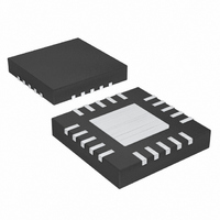
MAX5137GTG+ Maxim Integrated Products, MAX5137GTG+ Datasheet - Page 15

MAX5137GTG+
Manufacturer Part Number
MAX5137GTG+
Description
IC DAC 12BIT DUAL 1LSB 24-TQFN
Manufacturer
Maxim Integrated Products
Datasheet
1.MAX5137GTG.pdf
(19 pages)
Specifications of MAX5137GTG+
Settling Time
5µs
Number Of Bits
12
Data Interface
DSP, MICROWIRE™, QSPI™, Serial, SPI™
Number Of Converters
2
Voltage Supply Source
Analog and Digital
Power Dissipation (max)
2.22W
Operating Temperature
-40°C ~ 105°C
Mounting Type
Surface Mount
Package / Case
24-TQFN Exposed Pad
Resolution
12 bit
Interface Type
Serial (SPI)
Supply Voltage (max)
5.5 V
Supply Voltage (min)
2.7 V
Maximum Operating Temperature
+ 105 C
Mounting Style
SMD/SMT
Minimum Operating Temperature
- 40 C
Supply Current
2.3 mA
Voltage Reference
Internal or External
Lead Free Status / RoHS Status
Lead free / RoHS Compliant
Offset error indicates how well the actual transfer func-
tion matches the ideal transfer function at a single point.
Typically, the point at which the offset error is specified is
at or near the zero-scale point of the transfer function.
Gain error is the difference between the ideal and the
actual full-scale output voltage on the transfer curve,
after nullifying the offset error. This error alters the slope
of the transfer function and corresponds to the same
percentage error in each step.
The settling time is the amount of time required from the
start of a transition, until the DAC output settles to the new
output value within the converter’s specified accuracy.
Digital feedthrough is the amount of noise that appears
on the DAC output when the DAC digital control lines
are toggled.
TOP VIEW
*EXPOSED PAD.
**N.C. FOR THE MAX5136/MAX5137.
AVDD
REF0
GND
N.C.
REFI
N.C.
______________________________________________________________________________________
19
20
21
22
23
24
+
18
1
17
2
(4mm
Digital Feedthrough
THIN QFN
MAX5134–
MAX5137
16
3
×
4mm)
15
4
Settling Time
16-/12-Bit, Voltage-Output DACs
Offset Error
*EP
14
5
Gain Error
13
6
12
11
10
9
8
7
SCLK
N.C.
CS
DIN
N.C.
GND
Pin-/Software-Compatible,
A major carry transition occurs at the midscale point
where the MSB changes from low to high and all other
bits change from high to low, or where the MSB
changes from high to low and all other bits change from
low to high. The duration of the magnitude of the
switching glitch during a major carry transition is
referred to as the digital-to-analog glitch impulse.
The digital-to-analog power-up glitch is the duration of
the magnitude of the switching glitch that occurs as the
device exits power-down mode.
Crosstalk is the amount of noise that appears on a DAC
output set to 0 when the other DAC is updated from 0 to
AVDD
PROCESS: BiCMOS
Digital-to-Analog Power-Up Glitch Impulse
READY
DVDD
AVDD
OUT0
OUT3
GND
REFI
DIN
1
2
3
4
5
6
7
8
Digital-to-Analog Glitch Impulse
+
MAX5134–
MAX5137
TSSOP
DC DAC-to-DAC Crosstalk
Pin Configurations
Chip Information
16
15
14
13
12
11
10
9
REFO
GND
OUT1
M/Z
LDAC
OUT2**
SCLK
CS
15


