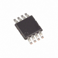
MAX5533EUA+ Maxim Integrated Products, MAX5533EUA+ Datasheet - Page 19

MAX5533EUA+
Manufacturer Part Number
MAX5533EUA+
Description
IC DAC 12BIT DUAL ULP 8-UMAX
Manufacturer
Maxim Integrated Products
Datasheet
1.MAX5532EUA.pdf
(24 pages)
Specifications of MAX5533EUA+
Settling Time
660µs
Number Of Bits
12
Data Interface
MICROWIRE™, QSPI™, Serial, SPI™
Number Of Converters
2
Voltage Supply Source
Single Supply
Power Dissipation (max)
471mW
Operating Temperature
-40°C ~ 85°C
Mounting Type
Surface Mount
Package / Case
8-MSOP, Micro8™, 8-uMAX, 8-uSOP,
Number Of Dac Outputs
2
Resolution
12 bit
Interface Type
Serial (SPI)
Supply Voltage (max)
5.5 V
Supply Voltage (min)
1.8 V
Maximum Operating Temperature
+ 85 C
Mounting Style
SMD/SMT
Minimum Operating Temperature
- 40 C
Supply Current
0.008 mA
Voltage Reference
Internal
Lead Free Status / RoHS Status
Lead free / RoHS Compliant
See the circuit in Figure 5 for an illustration of how to
configure the MAX5534/MAX5535 to bias a current-out-
put transducer. In Figure 5, the output voltage of the
MAX5534/MAX5535 is a function of the voltage drop
across the transducer added to the voltage drop
across the feedback resistor R.
Figure 6 shows the MAX5534 in a unipolar output con-
figuration with unity gain. Table 4 lists the unipolar out-
put codes.
The MAX5534 output can be configured for bipolar
operation as shown in Figure 7. The output voltage is
given by the following equation:
where N
binary input code. Table 5 shows the digital codes (off-
set binary) and the corresponding output voltage for
the circuit in Figure 7.
The MAX5534/MAX5535 have force-sense outputs,
which provide a connection directly to the inverting termi-
nal of the output op-amp, yielding the most flexibility. The
advantage of the force-sense output is that specific gains
can be set externally for a given application. The gain
error for the MAX5534/MAX5535 is specified in a unity-
gain configuration (op-amp output and inverting termi-
nals connected), and additional gain error results from
external resistor tolerances. Another advantage of the
force-sense DAC is that it allows many useful circuits to
be created with only a few simple external components.
An example of a custom fixed gain using the MAX5534/
MAX5535 force-sense output is shown in Figure 8. In
this example, R1 and R2 set the gain for V
Figure 6. Unipolar Output Circuit
REFIN
A
V
OUT_
MAX5534
represents the decimal value of the DAC’s
DAC
= V
______________________________________________________________________________________
REFIN
Current-Output Transducer
Configurable Output Gain
x [(N
A
- 2048) / 2048]
Voltage Biasing a
Unipolar Output
N
(0 TO 4095 DECIMAL).
V
FB_
OUT
A
Bipolar Output
IS THE DAC INPUT CODE
=
OUT_
V
REFIN
OUTA
4096
N
A
.
12-Bit, Voltage-Output DACs
where N
input code.
See the circuit in Figure 10 for an illustration of how to
use the MAX5535 to bias a two-electrode potentiostat
on the input of an ADC.
Bypass the power supply with a 0.1µF capacitor to GND.
Minimize lengths to reduce lead inductance. If noise
becomes an issue, use shielding and/or ferrite beads to
increase isolation. For the thin QFN package, connect the
exposed pad to ground.
Digital and AC transient signals coupling to GND can
create noise at the output. Use proper grounding tech-
niques, such as a multilayer board with a low-inductance
ground plane. Wire-wrapped boards and sockets are not
recommended. For optimum system performance, use
printed circuit (PC) boards. Good PC board ground lay-
out minimizes crosstalk between DAC outputs, reference
inputs, and digital inputs. Reduce crosstalk by keeping
analog lines away from digital lines.
Table 4. Unipolar Code Table (Gain = +1)
Table 5. Bipolar Code Table (Gain = +1)
Dual, Ultra-Low-Power,
MSB
1111
1000
1000
0111
0000
0000
MSB
1111
1000
1000
0111
0000
0000
V
OUTA
DAC CONTENTS
DAC CONTENTS
A
1111
0000
0000
1111
0000
0000
1111
0000
0000
1111
0000
0000
= [(V
represents the numeric value of the DAC
REFIN
1111
0001
0000
1111
0001
0000
1111
0001
0000
1111
0001
0000
LSB
LSB
Layout Considerations
Self-Biased Two-Electrode
x N
Bypassing Considerations
Potentiostat Application
A
) / 4096] x [1 + (R2 / R1)]
+V
-V
REF
REF
ANALOG OUTPUT
ANALOG OUTPUT
+V
+V
+V
+V
Power Supply and
-V
(2048/4096) = +V
+V
+V
-V
REF
(2048/2048) = -V
REF
REF
REF
REF
REF
REF
REF
(2047/2048)
(4095/4096)
(2049/4096)
(2047/4096)
(2047/2048)
0V
0V
(1/2048)
(1/4096)
(1/2048)
REF
REF
/ 2
19


