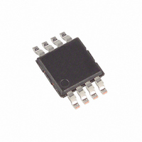
MAX5302CUA+ Maxim Integrated Products, MAX5302CUA+ Datasheet - Page 9

MAX5302CUA+
Manufacturer Part Number
MAX5302CUA+
Description
IC DAC 12BIT LP SERIAL 8-UMAX
Manufacturer
Maxim Integrated Products
Datasheet
1.MAX5302CUA.pdf
(12 pages)
Specifications of MAX5302CUA+
Settling Time
14µs
Number Of Bits
12
Data Interface
Serial
Number Of Converters
1
Voltage Supply Source
Single Supply
Operating Temperature
0°C ~ 70°C
Mounting Type
Surface Mount
Package / Case
8-MSOP, Micro8™, 8-uMAX, 8-uSOP,
Number Of Dac Outputs
1
Resolution
12 bit
Interface Type
Serial (SPI)
Supply Voltage (max)
5.5 V
Supply Voltage (min)
4.5 V
Maximum Operating Temperature
+ 70 C
Mounting Style
SMD/SMT
Minimum Operating Temperature
0 C
Supply Current
400 uA
Voltage Reference
External
Lead Free Status / RoHS Status
Lead free / RoHS Compliant
Power Dissipation (max)
-
Lead Free Status / Rohs Status
Lead free / RoHS Compliant
bits (C2, C1, C0), followed by the 12+1 data bits
D11...D0, S0 (Figure 4). Set the sub-bit (S0) to zero.
The 3-bit control code determines the register to be
updated and the configuration when exiting shutdown.
Figures 5 and 6 show the serial-interface timing require-
ments. The chip-select (CS) pin must be low to enable
the DAC’s serial interface. When CS is high, the inter-
face control circuitry is disabled. CS must go low at
least t
properly clock in the first bit. When CS is low, data is
clocked into the internal shift register through the serial-
data input pin (DIN) on SCLK’s rising edge. The maxi-
mum guaranteed clock frequency is 10MHz. Data is
latched into the MAX5302 input/DAC register on CS’s
rising edge.
Figure 7 shows a method of connecting several
MAX5302s. In this configuration, the clock and the data
bus are common to all devices, and separate chip-select
lines are used for each IC.
For a unipolar output, the output voltage and the refer-
ence input have the same polarity. Figure 8 shows the
MAX5302 unipolar output circuit, which is also the typical
operating circuit. Table 2 lists the unipolar output
codes.
Figure 8. Unipolar Output Circuit
Rail-to-Rail is a registered trademark of Nippon Motorola, Ltd.
CSS
before the rising serial-clock (SCLK) edge to
REF
Applications Information
DAC
_______________________________________________________________________________________
MAX5302
Low-Power, 12-Bit Voltage-Output DAC
V
+5V
DD
Unipolar Output
GND
FB
OUT
Figure 9 illustrates a Rail-to-Rail
shows the MAX5302 with the output amplifier configured
with a closed-loop gain of +2 to provide a 0V to 5V full-
scale range when a 2.5V reference is used.
The MAX5302 output can be configured for bipolar
operation using Figure 10’s circuit according to the fol-
lowing equation:
where NB is the numeric value of the DAC’s binary
input code. Table 3 shows digital codes (offset binary)
and the corresponding output voltage for Figure 10’s
circuit.
In applications where the reference has AC-signal com-
ponents, the MAX5302 has multiplying capability within
the reference input range specifications. Figure 11
shows a technique for applying a sine-wave signal to
the reference input where the AC signal is offset before
being applied to REF. The reference voltage must
never be more negative than GND.
The MAX5302’s total harmonic distortion plus noise
(THD+N) is typically less than -77dB (full-scale code),
given a 1Vp-p signal swing and input frequencies up to
25kHz. The typical -3dB frequency is 650kHz, as shown
in the Typical Operating Characteristics graphs.
Table 2. Unipolar Code Table
Note: ( ) are for sub-bit.
MSB
1 1 1 1 1 1 1 1 1 1 1 1 ( 0 )
1 0 0 0 0 0 0 0 0 0 0 1 ( 0 )
1 0 0 0 0 0 0 0 0 0 0 0 ( 0 )
0 1 1 1 1 1 1 1 1 1 1 1 ( 0 )
0 0 0 0 0 0 0 0 0 0 0 0 ( 0 )
0 0 0 0 0 0 0 0 0 0 0 1 ( 0 )
with Serial Interface
DAC CONTENTS
V
OUT
= V
LSB
REF
Using an AC Reference
[(2NB / 4096) - 1]
+V
REF
ANALOG OUTPUT
®
+V
+V
+V
+V
output. This circuit
Bipolar Output
2048
4096
REF
REF
REF
REF
0V
=
2049
4096
2047
4096
4096
4095
4096
1
+
V
REF
2
9


