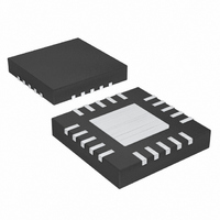
MAX5136AGTG+ Maxim Integrated Products, MAX5136AGTG+ Datasheet

MAX5136AGTG+
Specifications of MAX5136AGTG+
Related parts for MAX5136AGTG+
MAX5136AGTG+ Summary of contents
Page 1
... CMOS-Compatible Inputs with Hysteresis ♦ Low-Power Consumption (I PART MAX5134AGTG+ MAX5134AGUE+ MAX5135GTG+ MAX5135GUE+ Applications MAX5136AGTG+ MAX5136GUE+ MAX5137GTG+ MAX5137GUE+ + Denotes a lead(Pb)-free/RoHS-compliant package Exposed pad. Note: All devices are specified over the -40°C to +105°C oper- ating temperature range. Functional Diagrams, Pin Configurations, and Typical Operating Circuit appear at end of data sheet ...
Page 2
Pin-/Software-Compatible, 16-/12-Bit, Voltage-Output DACs ABSOLUTE MAXIMUM RATINGS AVDD to GND...........................................................-0.3V to +6V DVDD to GND...........................................................-0.3V to +6V OUT0–OUT3 to GND ....................................-0.3V to the lower of REFI, REFO, M/Z to GND .............................-0.3V to the lower of SCLK, DIN GND ...
Page 3
ELECTRICAL CHARACTERISTICS (continued 2.7V to 5.25V 2.7V to 5.25V, V AVDD DVDD unless otherwise noted. Typical values are MIN MAX PARAMETER SYMBOL DAC OUTPUT VOLTAGE (Note 2) ...
Page 4
Pin-/Software-Compatible, 16-/12-Bit, Voltage-Output DACs ELECTRICAL CHARACTERISTICS (continued 2.7V to 5.25V 2.7V to 5.25V, V AVDD DVDD unless otherwise noted. Typical values are MIN MAX PARAMETER SYMBOL POWER ...
Page 5
A A MAX5134/MAX5136 INTEGRAL NONLINEARITY vs. DIGITAL INPUT CODE 16384 32768 49152 65536 DIGITAL INPUT CODE (LSB) MAX5134/MAX5136 DIFFERENTIAL NONLINEARITY ...
Page 6
Pin-/Software-Compatible, 16-/12-Bit, Voltage-Output DACs (T = +25°C, unless otherwise noted.) A OFFSET ERROR vs. TEMPERATURE 0 -0 2.7V AVDD V = 2.5V REFI -0.2 -0.3 -0 5.25V AVDD -0 REFI -0.6 -40 -20 ...
Page 7
A SETTLING TIME DOWN MAX5134-MAX5137 toc19 500mV/div 400ns/div DIGITAL SUPPLY CURRENT vs. DIGITAL SUPPLY VOLTAGE 4 5.25V, SCLK = 0Hz AVDD 3.5 3.0 2.5 2.0 1.5 1.0 0.5 0 2.7 3.2 3.7 ...
Page 8
Pin-/Software-Compatible, 16-/12-Bit, Voltage-Output DACs (T = +25°C, unless otherwise noted.) A FULL-SCALE REFERENCE FEEDTHROUGH MAX5134-MAX5137 toc28 V OUT_ REF POWER-UP GLITCH, ZERO SCALE, EXTERNAL REFERENCE MAX5134-MAX5137 toc31 V AVDD V OUT_ POWER-UP GLITCH, MIDSCALE, INTERNAL REFERENCE V AVDD V OUT_ ...
Page 9
PIN MAX5134 MAX5136 MAX5135 MAX5137 TQFN-EP TSSOP TQFN-EP TSSOP 11, 14, 17, — 11, 13, 14 20, 23 17, 20 ...
Page 10
Pin-/Software-Compatible, 16-/12-Bit, Voltage-Output DACs when using the internal reference. Bypass REFO to GND with a 47pF (maximum 100pF) capacitor. Alternatively, if heavier decoupling is required, use a 1kΩ resistor in series with a 1µF capacitor in parallel with the existing ...
Page 11
The MAX5134–MAX5137 digital inputs are double buffered. Depending on the command issued through the serial interface, the input register(s) can be loaded without affecting the DAC register(s) using the write command. To update the DAC registers, either pulse the LDAC ...
Page 12
Pin-/Software-Compatible, 16-/12-Bit, Voltage-Output DACs Connect READY to a microcontroller (µC) input to moni- tor the serial interface for valid communications. The READY pulse appears 24 clock cycles after the nega- tive edge of CS (Figure 4). Since the MAX5134– MAX5137 ...
Page 13
CSm μC CS1 CS SCLK DWRITE DREAD INT Figure 6. Daisy Chain (CS Not Used) ______________________________________________________________________________________ Pin-/Software-Compatible, 16-/12-Bit, Voltage-Output DACs TO OTHER CHIPS/CHAINS SLAVE 1 CS MAX5134– SCLK MAX5137 DIN READY SLAVE 2 CS MAX5134– SCLK MAX5137 DIN READY SLAVE ...
Page 14
Pin-/Software-Compatible, 16-/12-Bit, Voltage-Output DACs LDAC OUT_ Figure 7. Output Timing Applications Information Power-On Reset (POR) On power-up, the input registers are set to zero, DAC outputs power up to zero or midscale, depending on the configuration of M/Z. Connect M/Z ...
Page 15
Offset error indicates how well the actual transfer func- tion matches the ideal transfer function at a single point. Typically, the point at which the offset error is specified near the zero-scale point of the transfer function. ...
Page 16
Pin-/Software-Compatible, 16-/12-Bit, Voltage-Output DACs MAX5134 MAX5135 M/Z CS SERIAL-TO- SCLK PARALLEL CONVERTER DIN READY 16 ______________________________________________________________________________________ AVDD DVDD GND POR POWER-DOWN CONTROL CONTROL LOGIC INPUT DAC REGISTER REGISTER DAC INPUT REGISTER REGISTER INPUT DAC REGISTER REGISTER DAC INPUT REGISTER REGISTER ...
Page 17
Voltage-Output DACs POR MAX5136 MAX5137 M/Z CONTROL LOGIC INPUT CS REGISTER SERIAL-TO- SCLK PARALLEL CONVERTER DIN INPUT REGISTER READY ______________________________________________________________________________________ Pin-/Software-Compatible, Functional Diagrams (continued) AVDD DVDD GND REFI REFO REFERENCE POWER-DOWN CONTROL DAC 12-/16-BIT REGISTER DAC DAC 12-/16-BIT REGISTER ...
Page 18
Pin-/Software-Compatible, 16-/12-Bit, Voltage-Output DACs DIGITAL POWER SUPPLY 100nF NOTE: SHOWN IN BIPOLAR CONFIGURATION. For the latest package outline information and land patterns www.maxim-ic.com/packages. Note that a “+”, “#”, or “-” in the package code indicates RoHS status only. ...
Page 19
... Maxim cannot assume responsibility for use of any circuitry other than circuitry entirely embodied in a Maxim product. No circuit patent licenses are implied. Maxim reserves the right to change the circuitry and specifications without notice at any time. Maxim Integrated Products, 120 San Gabriel Drive, Sunnyvale, CA 94086 408-737-7600 ____________________ 19 © 2010 Maxim Integrated Products ...


