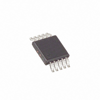
MAX552AEUB+ Maxim Integrated Products, MAX552AEUB+ Datasheet - Page 11

MAX552AEUB+
Manufacturer Part Number
MAX552AEUB+
Description
IC DAC 12BIT QUAD SER 10-UMAX
Manufacturer
Maxim Integrated Products
Datasheet
1.MAX552AEUB.pdf
(12 pages)
Specifications of MAX552AEUB+
Settling Time
120ns
Number Of Bits
12
Data Interface
Serial
Number Of Converters
1
Voltage Supply Source
Single Supply
Power Dissipation (max)
444mW
Operating Temperature
-40°C ~ 85°C
Mounting Type
Surface Mount
Package / Case
10-MSOP, Micro10™, 10-uMAX, 10-uSOP
Resolution
12 bit
Interface Type
Serial (SPI)
Supply Voltage (max)
3.6 V
Supply Voltage (min)
2.7 V
Maximum Operating Temperature
+ 85 C
Mounting Style
SMD/SMT
Minimum Operating Temperature
- 40 C
Supply Current
0.005 mA
Voltage Reference
External
Lead Free Status / RoHS Status
Lead free / RoHS Compliant
An advantage of voltage mode operation is that a neg-
ative reference is not required for a positive output.
Note that the reference input (OUT) must always be
positive and is limited to no more than 2V when V
5V. The unipolar and bipolar circuits in Figures 3 and 4
can be converted to voltage mode.
Figure 6 shows the MAX551/MAX552 in a current out-
put configuration in which the output amplifier is pow-
ered from a single supply, and AGND is biased to
1.23V. With 0V applied to the REF input, the output can
be programmed from 1.23V (zero code) to 2.46V (full
scale). With 2.45V applied to REF, the output can be
programmed from 1.23V (zero code) to 0.01V (full
scale).
The MAX4166 op amp that drives AGND maintains the
1.23V bias as AGND’s impedance changes with the
DAC’s digital code, from high impedance (zero code)
to 7kΩ minimum (full scale).
In applications where reference voltage has AC signal
components, the MAX551/MAX552 have multiplying
capability within the reference input range of ±6V. If the
DAC and the output amplifier are operated with a single
Figure 6. Single-Supply, Current Mode Operation
+1.43V TO +12.6V
MAX6160
+5V (+3V)
REF
DGND
OUT
ADJ
V
DD
MAX551
MAX552
+3V/+5V, 12-Bit, Serial, Multiplying DACs
______________________________________________________________________________________
106MΩ
MAX4167
RFB
AGND
OUT
Using an AC Reference
( ) ARE FOR MAX552
C1
MAX4167
Current Mode
DD
V
OUT
is
in 10-Pin µMAX Package
supply voltage, then an AC reference input can be off-
set with the circuit shown in Figure 7 to prevent the
DAC output voltage from exceeding the output amplifi-
er’s negative output rail. The reference input’s typical
-3dB bandwidth is greater than 700kHz, as shown in
the Typical Operating Characteristics graphs.
The MAX551/MAX552 provide separate AGND and
GND inputs in the µMAX package. With this package,
AGND can be biased above GND to provide an arbi-
trary nonzero output voltage for a “0” input code
(Figure 8).
Bypass V
V
and GND) should be connected in a star configuration
to the highest quality ground available, which should be
located as close to the MAX551/MAX552 as possible.
Since OUT and the output amplifier’s noninverting input
are sensitive to offset voltage, nodes that are to be
grounded should be connected directly to a single-
point ground through a separate, low-resistance (less
than 0.2Ω) connection. The current at OUT and AGND
varies with input code, creating a code-dependent
error if these terminals are connected to ground (or vir-
tual ground) through a resistive path.
Parasitic coupling of the signal from REF to OUT is an
error source in dynamic applications. This coupling is
normally a function of board layout and pin-to-pin pack-
age capacitance. Minimize digital feedthrough with
guard traces between digital inputs, REF, and OUT
pins.
Figure 7. Single-Supply AC Reference Input Circuit
DD
REFERENCE
( ) ARE FOR MAX552
and GND as possible. The ground pins (AGND
(+3V)
+5V
INPUT
AC
DD
Layout, Grounding, and Bypassing
with a 0.1µF capacitor, located as close to
10kΩ
10kΩ
MAX4166
Offsetting AGND
GND
REF
MAX551
MAX552
V
DD
OUT
11


