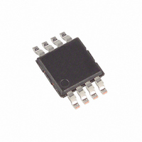
MAX5352BEUA+ Maxim Integrated Products, MAX5352BEUA+ Datasheet - Page 10

MAX5352BEUA+
Manufacturer Part Number
MAX5352BEUA+
Description
IC DAC 12BIT VOLT OUT SER 8-UMAX
Manufacturer
Maxim Integrated Products
Datasheet
1.MAX5352BCPA.pdf
(16 pages)
Specifications of MAX5352BEUA+
Settling Time
14µs
Number Of Bits
12
Data Interface
Serial
Number Of Converters
1
Voltage Supply Source
Single Supply
Power Dissipation (max)
330mW
Operating Temperature
-40°C ~ 85°C
Mounting Type
Surface Mount
Package / Case
8-MSOP, Micro8™, 8-uMAX, 8-uSOP,
Number Of Dac Outputs
1
Resolution
12 bit
Interface Type
Serial (SPI)
Supply Voltage (max)
5.5 V
Supply Voltage (min)
4.5 V
Maximum Operating Temperature
+ 85 C
Mounting Style
SMD/SMT
Minimum Operating Temperature
- 40 C
Supply Current
400 uA
Voltage Reference
External
Lead Free Status / RoHS Status
Lead free / RoHS Compliant
Low-Power, 12-Bit Voltage-Output DACs
with Serial Interface
to recall the output state prior to entering shutdown.
Exit shutdown mode by either recalling the previous
configuration or by updating the DAC with new data.
When powering up the device or bringing it out of shut-
down, allow 20µs for the output to stabilize.
The MAX5352/MAX5353’s 3-wire serial interface is
compatible with both Microwire™ (Figure 2) and
SPI™/QSPI™ (Figure 3). The serial input word consists
of three control bits followed by 12+1 data bits (MSB
first), as shown in Figure 4. The 3-bit control code
determines the MAX5352/MAX5353’s response outlined
in Table 1.
The MAX5352/MAX5353’s digital inputs are double
buffered. Depending on the command issued through
the serial interface, the input register can be loaded
without affecting the DAC register, the DAC register
can be loaded directly, or the DAC register can be
updated from the input register (Table 1).
The +3.3V MAX5353 can also directly interface with
+5V logic.
The MAX5352/MAX5353 require 16 bits of serial data.
Table 1 lists the serial-interface programming com-
mands. For certain commands, the 12+1 data bits are
“don’t cares.” Data is sent MSB first and can be sent in
two 8-bit packets or one 16-bit word (CS must remain
low until 16 bits are transferred). The serial data is com-
posed of three control bits (C2, C1, C0), followed by
the 12+1 data bits D11...D0, S0 (Figure 4). Set the
sub-bit (S0) to zero. The 3-bit control code determines:
Figure 5 shows the serial-interface timing requirements.
The chip-select pin (CS) must be low to enable the
DAC’s serial interface. When CS is high, the interface
control circuitry is disabled. CS must go low at least
t
erly clock in the first bit. When CS is low, data is
clocked into the internal shift register via the serial-data
input pin (DIN) on SCLK’s rising edge. The maximum
guaranteed clock frequency is 10MHz. Data is latched
into the MAX5352/MAX5353 input/DAC register on CS’s
rising edge.
10
CSS
______________________________________________________________________________________
the register to be updated,
the configuration when exiting shutdown.
before the rising serial clock (SCLK) edge to prop-
Serial-Interface Configurations
Serial-Interface Description
Figure 2. Connections for Microwire
Figure 3. Connections for SPI/QSPI
Figure 4. Serial-Data Format
MSB ..................................................................................LSB
C2
3 Control
Control
MAX5352
MAX5353
MAX5352
MAX5353
Bits
Bits
C1
C0
SCLK
SCLK
DIN
DIN
16 Bits of Serial Data
CS
CS
MSB ................................LSB Sub-Bit
D11 .....................................D0, S0
12+1 Data Bits
CPOL = 0, CPHA = 0
Data Bits
SK
SO
I/O
MOSI
SCK
I/O
MICROWIRE
SPI/QSPI
PORT
PORT
+5V
SS


