MAX5183BEEI+ Maxim Integrated Products, MAX5183BEEI+ Datasheet - Page 2
MAX5183BEEI+
Manufacturer Part Number
MAX5183BEEI+
Description
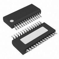
IC DAC 10BIT 40MHZ DUAL 28-QSOP
Manufacturer
Maxim Integrated Products
Datasheet
1.MAX5183BEEI.pdf
(14 pages)
Specifications of MAX5183BEEI+
Settling Time
25µs
Number Of Bits
10
Data Interface
Parallel
Number Of Converters
2
Voltage Supply Source
Analog and Digital
Operating Temperature
-40°C ~ 85°C
Mounting Type
Surface Mount
Package / Case
28-QSOP
Number Of Dac Outputs
2
Resolution
10 bit
Interface Type
Parallel
Supply Voltage (max)
3.3 V
Supply Voltage (min)
2.7 V
Maximum Operating Temperature
+ 85 C
Mounting Style
SMD/SMT
Maximum Power Dissipation
725 mW
Minimum Operating Temperature
- 40 C
Supply Current
4.2 mA
Lead Free Status / RoHS Status
Lead free / RoHS Compliant
Power Dissipation (max)
-
Lead Free Status / Rohs Status
Lead free / RoHS Compliant


ABSOLUTE MAXIMUM RATINGS
AV
Digital Inputs to DGND.............................................-0.3V to +6V
OUT1P, OUT1N, OUT2P, OUT2N, CREF1,
V
AGND to DGND.....................................................-0.3V to +0.3V
AV
ELECTRICAL CHARACTERISTICS
(AV
unless otherwise noted. Typical values are at T
Dual, 10-Bit, 40MHz, Current/Voltage
Simultaneous-Output DACs
Stresses beyond those listed under “Absolute Maximum Ratings” may cause permanent damage to the device. These are stress ratings only, and functional
operation of the device at these or any other conditions beyond those indicated in the operational sections of the specifications is not implied. Exposure to
absolute maximum rating conditions for extended periods may affect device reliability.
2
REF
DYNAMIC PERFORMANCE
ANALOG OUTPUT
Resolution
Integral Nonlinearity
Differential Nonlinearity
Zero-Scale Error
Full-Scale Error
Output Settling Time
Glitch Impulse
Spurious-Free Dynamic Range
to Nyquist
Total Harmonic Distortion to
Nyquist
Signal-to-Noise Ratio to Nyquist
DAC-to-DAC Output Isolation
Clock and Data Feedthrough
Output Noise
Gain Mismatch Between
DAC Outputs
Phase Mismatch Between
DAC Outputs
Full-Scale Output Voltage
Voltage Compliance of Output
Output Leakage Current
Full-Scale Output Current
DAC External Output Resistor
Load
CREF2 to AGND ...................................................-0.3V to +6V
DD
DD
DD
_______________________________________________________________________________________
to AGND ..........................................................-0.3V to +6V
, DV
to DV
= DV
DD
PARAMETER
DD
DD
to AGND, DGND .................................-0.3V to +6V
.................................................................... ±3.3V
= 3V ±10%, AGND = DGND = 0, f
SYMBOL
SFDR
DNL
THD
SNR
INL
V
I
R
N
FS
FS
L
A
Guaranteed monotonic
MAX5180
MAX5183
(Note 1)
To ±0.5LSB error band
f
f
f
f
All 0s to all 1s
f
f
DACEN = 0, MAX5180 only
MAX5180 only
MAX5180 only
CLK
CLK
CLK
OUT
OUT
OUT
= +25°C.)
CLK
= 40MHz
= 40MHz
= 40MHz
= 2.2MHz
= 2.2MHz, T
= 2.2MHz
= 40MHz, I
CONDITIONS
A
f
f
f
f
f
f
OUT
OUT
OUT
OUT
OUT
OUT
FS
=+25°C
Maximum Current into Any Pin............................................50mA
Continuous Power Dissipation (T
Operating Temperature Range
Storage Temperature Range .............................-65°C to +150°C
Lead Temperature (soldering, 10s) ................................ +300°C
= 1mA, 400Ω differential output, C
= 550kHz
= 2.2MHz, T
= 550kHz
= 2.2MHz, T
= 550kHz
= 2.2MHz, T
28-Pin QSOP (derate 9.00mW/°C above +70°C)....... 725mW
MAX518_BEEI.................................................-40°C to +85°C
A
A
A
=+25°C
=+25°C
=+25°C
MIN
-0.3
-40
0.5
10
57
-2
-1
-2
-8
-1
A
= +70°C)
L
= 5pF, T
±0.15
±0.5
±0.5
±0.5
TYP
±15
400
400
-70
-68
-60
25
10
72
70
61
59
50
10
1
A
MAX
+40
= T
-63
0.8
1.5
+2
+1
+2
+8
±1
1
MIN
degrees
pA/√Hz
to T
UNITS
%FSR
pV-s
LSB
LSB
LSB
LSB
dBc
dBc
Bits
nVs
mA
mV
dB
dB
µA
ns
Ω
V
MAX
,
Related parts for MAX5183BEEI+
Image
Part Number
Description
Manufacturer
Datasheet
Request
R

Part Number:
Description:
MAX7528KCWPMaxim Integrated Products [CMOS Dual 8-Bit Buffered Multiplying DACs]
Manufacturer:
Maxim Integrated Products
Datasheet:
Part Number:
Description:
Single +5V, fully integrated, 1.25Gbps laser diode driver.
Manufacturer:
Maxim Integrated Products
Datasheet:
Part Number:
Description:
Single +5V, fully integrated, 155Mbps laser diode driver.
Manufacturer:
Maxim Integrated Products
Datasheet:
Part Number:
Description:
VRD11/VRD10, K8 Rev F 2/3/4-Phase PWM Controllers with Integrated Dual MOSFET Drivers
Manufacturer:
Maxim Integrated Products
Datasheet:
Part Number:
Description:
Highly Integrated Level 2 SMBus Battery Chargers
Manufacturer:
Maxim Integrated Products
Datasheet:
Part Number:
Description:
Current Monitor and Accumulator with Integrated Sense Resistor; ; Temperature Range: -40°C to +85°C
Manufacturer:
Maxim Integrated Products
Part Number:
Description:
TSSOP 14/A�/RS-485 Transceivers with Integrated 100O/120O Termination Resis
Manufacturer:
Maxim Integrated Products
Part Number:
Description:
TSSOP 14/A�/RS-485 Transceivers with Integrated 100O/120O Termination Resis
Manufacturer:
Maxim Integrated Products
Part Number:
Description:
QFN 16/A�/AC-DC and DC-DC Peak-Current-Mode Converters with Integrated Step
Manufacturer:
Maxim Integrated Products
Part Number:
Description:
TDFN/A/65V, 1A, 600KHZ, SYNCHRONOUS STEP-DOWN REGULATOR WITH INTEGRATED SWI
Manufacturer:
Maxim Integrated Products
Part Number:
Description:
Integrated Temperature Controller f
Manufacturer:
Maxim Integrated Products
Part Number:
Description:
SOT23-6/I�/45MHz to 650MHz, Integrated IF VCOs with Differential Output
Manufacturer:
Maxim Integrated Products
Part Number:
Description:
SOT23-6/I�/45MHz to 650MHz, Integrated IF VCOs with Differential Output
Manufacturer:
Maxim Integrated Products
Part Number:
Description:
EVALUATION KIT/2.4GHZ TO 2.5GHZ 802.11G/B RF TRANSCEIVER WITH INTEGRATED PA
Manufacturer:
Maxim Integrated Products
Part Number:
Description:
QFN/E/DUAL PCIE/SATA HIGH SPEED SWITCH WITH INTEGRATED BIAS RESISTOR
Manufacturer:
Maxim Integrated Products
Datasheet: