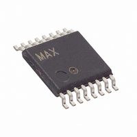
MAX5307EUE+ Maxim Integrated Products, MAX5307EUE+ Datasheet - Page 2

MAX5307EUE+
Manufacturer Part Number
MAX5307EUE+
Description
IC DAC 12BIT OCT LP SER 16-TSSOP
Manufacturer
Maxim Integrated Products
Datasheet
1.MAX5307EUE.pdf
(15 pages)
Specifications of MAX5307EUE+
Settling Time
5µs
Number Of Bits
12
Data Interface
Serial
Number Of Converters
8
Voltage Supply Source
Single Supply
Operating Temperature
-40°C ~ 85°C
Mounting Type
Surface Mount
Package / Case
16-TSSOP
Number Of Dac Outputs
8
Resolution
12 bit
Interface Type
Serial (SPI)
Supply Voltage (max)
5.5 V
Supply Voltage (min)
2.7 V
Maximum Operating Temperature
+ 85 C
Mounting Style
SMD/SMT
Minimum Operating Temperature
- 40 C
Supply Current
1.7 mA
Voltage Reference
External
Lead Free Status / RoHS Status
Lead free / RoHS Compliant
Power Dissipation (max)
-
Lead Free Status / Rohs Status
Lead free / RoHS Compliant
ABSOLUTE MAXIMUM RATINGS
V
All Other Pins to GND.................................-0.3V to (V
Continuous Power Dissipation (T
Low-Power, Low-Glitch, Octal 12-Bit Voltage-
Output DACs with Serial Interface
Stresses beyond those listed under “Absolute Maximum Ratings” may cause permanent damage to the device. These are stress ratings only, and functional
operation of the device at these or any other conditions beyond those indicated in the operational sections of the specifications is not implied. Exposure to
absolute maximum rating conditions for extended periods may affect device reliability.
ELECTRICAL CHARACTERISTICS
(V
at V
2
STATIC ACCURACY (Notes 1, 2)
Resolution
Integral Nonlinearity
Differential Nonlinearity
Offset Error (Note 3)
Offset Error Temperature Coefficient
Gain Error (Note 3)
Gain Error Temperature Coefficient
REFERENCE INPUT
Reference Input Voltage Range (Note 4)
Reference Input Impedance
Reference Current
DAC OUTPUTS
Output Voltage Range
DC Output Impedance
Capacitive Load
Resistive Load
Short-Circuit Current
Wake-Up Time
DD
DD
16-Pin TSSOP (derate 9.4mW/°C above +70°C) .........775mW
DD
_______________________________________________________________________________________
to GND ............................................................. -0.3V to +6V
= +2.7V to +5.5V, GND = 0, V
= +5V, T
PARAMETER
A
= +25°C.)
A
= +70°C)
REF
= V
DD
, C
SYMBOL
R
I
L
REFPD
V
DNL
V
V
REFIN
= 200pF, R
INL
C
R
REF
N
OE
GE
L
L
DD
+ 0.3V)
Guaranteed monotonic
In power-down mode
With no load
V
V
From shutdown mode
DD
DD
L
= 2kΩ, T
= +5V
= +2.7V
CONDITIONS
Maximum Current Into Any Pin .........................................±50mA
Operating Temperature Range ...........................-40°C to +85°C
Junction Temperature ......................................................+150°C
Storage Temperature Range .............................-65°C to +150°C
Lead Temperature (soldering, 10s) .................................+300°C
A
= T
MIN
to T
MAX
, unless otherwise noted. Typical values are
0.020
MIN
135
0.8
12
±0.1
TYP
±10
±10
200
500
0.5
±1
±5
33
20
24
1
2
0.020
V
MAX
±1.0
V
±60
265
±4
DD
±1
10
DD
-
% of FS
ppm/°C
UNITS
µV/°C
LSB
LSB
Bits
mV
mA
kΩ
kΩ
µA
pF
µs
Ω
V
V


