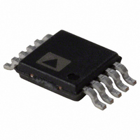
AD5623RBRMZ-5 Analog Devices Inc, AD5623RBRMZ-5 Datasheet - Page 25

AD5623RBRMZ-5
Manufacturer Part Number
AD5623RBRMZ-5
Description
IC DAC NANO 12BIT DUAL 10-MSOP
Manufacturer
Analog Devices Inc
Series
nanoDAC™r
Specifications of AD5623RBRMZ-5
Data Interface
Serial
Settling Time
3µs
Number Of Bits
12
Number Of Converters
2
Voltage Supply Source
Single Supply
Power Dissipation (max)
5mW
Operating Temperature
-40°C ~ 105°C
Mounting Type
Surface Mount
Package / Case
10-MSOP, Micro10™, 10-uMAX, 10-uSOP
Resolution (bits)
12bit
Sampling Rate
287kSPS
Input Channel Type
Serial
Supply Voltage Range - Analog
2.7V To 3.6V, 4.5V To 5.5V
Supply Current
800µA
Lead Free Status / RoHS Status
Lead free / RoHS Compliant
Available stocks
Company
Part Number
Manufacturer
Quantity
Price
Part Number:
AD5623RBRMZ-5
Manufacturer:
ADI/亚德诺
Quantity:
20 000
Part Number:
AD5623RBRMZ-5REEL
Manufacturer:
ADI/亚德诺
Quantity:
20 000
Company:
Part Number:
AD5623RBRMZ-5REEL7
Manufacturer:
TOSHIBA
Quantity:
5 000
MICROPROCESSOR INTERFACING
AD5623R/AD5643R/AD5663R to Blackfin® ADSP-BF53X
Interface
Figure 56 shows a serial interface between the AD5623R/
AD5643R/AD5663R and the
processor. The ADSP-BF53X processor family incorporates two
dual-channel synchronous serial ports, SPORT1 and SPORT0,
for serial and multiprocessor communications. Using SPORT0
to connect to the AD5623R/AD5643R/AD5663R, the setup for
the interface is as follows: DT0PRI drives the DIN pin of the
AD5623R/AD5643R/AD5663R, while TSCLK0 drives the
SCLK of the parts. The SYNC is driven from TFS0.
AD5623R/AD5643R/AD5663R to 68HC11/68L11
Interface
Figure 57 shows a serial interface between the AD5623R/
AD5643R/AD5663R and the 68HC11/68L11 microcontroller.
SCK of the 68HC11/68L11 drives the SCLK of the AD5623R/
AD5643R/AD5663R, and the MOSI output drives the serial
data line of the DAC.
The SYNC signal is derived from a port line (PC7). The setup
conditions for correct operation of this interface are as follows:
the 68HC11/68L11 is configured with its CPOL bit as 0, and its
CPHA bit as 1. When data is being transmitted to the DAC, the
SYNC line is taken low (PC7). When the 68HC11/68L11 is
configured as described previously, data appearing on the MOSI
output is valid on the falling edge of SCK. Serial data from the
68HC11/68L11 is transmitted in 8-bit bytes with only eight
falling clock edges occurring in the transmit cycle.
Figure 56. AD5623R/AD5643R/AD5663R to Blackfin ADSP-BF53X Interface
Figure 57. AD5623R/AD5643R/AD5663R to 68HC11/68L11 Interface
1
1
ADDITIONAL PINS OMITTED FOR CLARITY.
68HC11/68L11
ADDITIONAL PINS OMITTED FOR CLARITY.
ADSP-BF53x
TSCLK0
DTOPRI
TFS0
MOSI
SCK
PC7
1
1
Blackfin ADSP-BF53X
SYNC
DIN
SCLK
AD5663R
AD5643R/
SYNC
SCLK
DIN
AD5663R
AD5643R/
1
1
micro-
Rev. C | Page 25 of 28
Data is transmitted MSB first. To load data to the AD5623R/
AD5643R/AD5663R, PC7 is left low after the first eight bits are
transferred, and a second serial write operation is performed to
the DAC. PC7 is taken high at the end of this procedure.
AD5623R/AD5643R/AD5663R to 80C51/80L51 Interface
Figure 58 shows a serial interface between the AD5623R/
AD5643R/AD5663R and the 80C51/80L51 microcontroller.
The setup for the interface is as follows: TxD of the 80C51/
80L51 drives SCLK of the AD5623R/AD5643R/AD5663R,
and RxD drives the serial data line of the part. The SYNC signal
is again derived from a bit-programmable pin on the port. In this
case, Port Line P3.3 is used. When data is to be transmitted to the
AD5623R/AD5643R/AD5663R, P3.3 is taken low. The 80C51/
80L51 transmit data in 8-bit bytes only; thus, only eight falling
clock edges occur in the transmit cycle. To load data to the
DAC, P3.3 is left low after the first eight bits are transmitted,
and a second write cycle is initiated to transmit the second byte
of data. P3.3 is taken high following the completion of this cycle.
The 80C51/80L51 output the serial data in a format that has the
LSB first. The AD5623R/AD5643R/AD5663R must receive data
with the MSB first. The 80C51/80L51 transmit routine should
take this into account.
AD5623R/AD5643R/AD5663R to MICROWIRE Interface
Figure 59 shows an interface between the AD5623R/AD5643R/
AD5663R and any MICROWIRE-compatible device. Serial data is
shifted out on the falling edge of the serial clock and is clocked into
the AD5623R/AD5643R/AD5663R on the rising edge of the SK.
Figure 58. AD5623R/AD5643R/AD5663R to 80C512/80L51 Interface
Figure 59. AD5623R/AD5643R/AD5663R to MICROWIRE Interface
1
1
ADDITIONAL PINS OMITTED FOR CLARITY.
ADDITIONAL PINS OMITTED FOR CLARITY.
80C51/80L51
MICROWIRE
AD5623R/AD5643R/AD5663R
P3.3
RxD
TxD
CS
SK
SO
1
1
SYNC
SCLK
DIN
SYNC
SCLK
DIN
AD5663R
AD5663R
AD5643R/
AD5643R/
1
1


