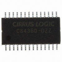
CS4360-DZZ Cirrus Logic Inc, CS4360-DZZ Datasheet - Page 27

CS4360-DZZ
Manufacturer Part Number
CS4360-DZZ
Description
IC DAC STER 6CH 102DB 28TSSOP
Manufacturer
Cirrus Logic Inc
Datasheet
1.CS4360-KZZ.pdf
(37 pages)
Specifications of CS4360-DZZ
Data Interface
Serial
Number Of Bits
24
Number Of Converters
6
Voltage Supply Source
Analog and Digital
Power Dissipation (max)
265mW
Operating Temperature
-40°C ~ 85°C
Mounting Type
Surface Mount
Package / Case
28-TSSOP
Resolution (bits)
24bit
Sampling Rate
192kSPS
Input Channel Type
Serial
Supply Current
25mA
Digital Ic Case Style
TSSOP
No. Of Pins
28
Lead Free Status / RoHS Status
Lead free / RoHS Compliant
Settling Time
-
Lead Free Status / RoHS Status
Lead free / RoHS Compliant, Lead free / RoHS Compliant
Other names
598-1056-5
Available stocks
Company
Part Number
Manufacturer
Quantity
Price
Company:
Part Number:
CS4360-DZZ
Manufacturer:
Cirrus Logic Inc
Quantity:
135
Company:
Part Number:
CS4360-DZZR
Manufacturer:
CIRRUS
Quantity:
4 000
4.9.2b
To read from the device, follow the procedure below while adhering to the control port Switching Specifi-
cations. During this operation it is first necessary to write to the device, specifying the appropriate register
through the MAP.
1) After writing to the MAP (see section 4.9.1), initiate a repeated START condition to the I²C bus fol-
2) Signal the end of the address byte by not issuing an acknowledge. The device will then transmit the
3) If the INCR bit is set to 1, the device will continue to transmit the contents of successive registers. Con-
4) If the INCR bit is set to 0 and further I²C reads from other registers are desired, it is necessary to repeat
4.9.3
In SPI mode, data is clocked into the serial control data line, CDIN, by the serial control port clock, CCLK
(see Figure 21 for the clock to data relationship). There is no AD0 pin. Pin CS is the chip select signal and
is used to control SPI writes to the control port. When the device detects a high-to-low transition on the
AD0/CS pin after power-up, SPI mode will be selected. All signals are inputs and data is clocked in on the
rising edge of CCLK.
DS517F2
S D A
S C L
lowed by the address byte. The upper 6 bits must be 001000. The seventh bit must match the setting
of the AD0 pin, and the eighth must be 1. The eighth bit of the address byte is the R/W bit.
contents of the register pointed to by the MAP. The MAP will contain the address of the last register
written to the MAP.
tinue providing a clock but do not issue an ACK on the bytes clocked out of the device. After all the
desired registers are read, initiate a STOP condition to the bus.
the procedure detailed from step 1. If no further reads from other registers are desired, initiate a STOP
condition to the bus.
S ta rt
SPI Mode
I²C Read
0 0 1 0 0 0
S D A
S C L
A D 0
S ta rt
W
0 01 00 0
A C K
A D 0
M A P
1 - 8
W
Figure 19. I²C Write
A C K
Figure 20. I²C Read
R ep e a te d S T A R T
A b o rte d W R IT E
A C K
o r
M A P
0 0 1 0 0 0
1 -8
A D 0
A C K
R
D A TA
1-8
A C K
A C K
(po in te d to b y M A P )
D a ta 1 -8
S top
A C K
(p oin te d to b y M A P )
D a ta 1 -8
CS4360
S to p
27


