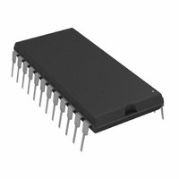
ADDAC80NZ-CBI-V Analog Devices Inc, ADDAC80NZ-CBI-V Datasheet - Page 11

ADDAC80NZ-CBI-V
Manufacturer Part Number
ADDAC80NZ-CBI-V
Description
IC DAC 12-BIT BINARY MONO 24-DIP
Manufacturer
Analog Devices Inc
Datasheet
1.ADDAC80NZ-CBI-V.pdf
(16 pages)
Specifications of ADDAC80NZ-CBI-V
Data Interface
Parallel
Settling Time
2µs
Number Of Bits
12
Number Of Converters
1
Voltage Supply Source
Dual ±
Power Dissipation (max)
300mW
Operating Temperature
0°C ~ 70°C
Mounting Type
Through Hole
Package / Case
24-DIP (0.600", 15.24mm)
Resolution (bits)
12bit
Input Channel Type
Parallel
Supply Current
20mA
Digital Ic Case Style
DIP
No. Of Pins
24
Operating Temperature Range
0°C To +70°C
Msl
MSL 3 - 168 Hours
Lead Free Status / RoHS Status
Lead free / RoHS Compliant
DRIVING A RESISTIVE LOAD UNIPOLAR
A load resistance, R
Figure 12 will generate a voltage range, V
where R
To achieve specified drift, connect the internal scaling resistor
(R
(R
With R
VOLTAGE OUTPUT MODELS
Internal scaling resistors provided in the ADDAC80 may be
connected to produce bipolar output voltage ranges of ± 10 V,
± 5 V or ± 2.5 V or unipolar output voltage ranges of 0 V to +5 V
or 0 V to +10 V (see Figure 9).
Gain and offset drift are minimized in the ADDAC80 because
of the thermal tracking of the scaling resistors with other device
components. Connections for various output voltage ranges are
shown in Table III. Settling time is specified for a full-scale
range change: 4 s for a 10 kΩ feedback resistor; 3 s for a 5 kΩ
feedback resistor when using the compensation capacitor shown
in Figure 3a.
The equivalent resistive scaling network and output circuit of
the current model are shown in Figures 10 and 11. External R
resistors are required to produce exactly 0 V to –2 V or ± 1 V
output. TCR of these resistors should be ± 100 ppm/°C or less
to maintain the ADDAC80 output specifications. If exact output
ranges are not required, the external resistors are not needed.
V
LI
LS
WEIGHTED
NETWORK
RESISTOR
CONTROL
OUT
) as shown in Table IV to an external metal film trim resistor
) to provide full scale output voltage range of 0 V to –2 V.
CIRCUIT
TO REF
FROM
LS
L
=
max = 1.54 kΩ and V
= 0 V, V
–
2
mA
JUNCTION
SUMMING
OUT
INPUT
6 6
6 6
REF
16
20
.
.
L
= R
= –1.69 V.
k
k
+
–
Ω
Ω
LI
×
+
5k
Output
Range
± 10 V
± 5 V
± 2.5 V
0 V to 10 V
0 V to 5 V
0 V to 10 V
NC = No Connect
, + R
R
R
L
L
OUT
Table III. Output Voltage Range Connections, Voltage Model ADDAC80
LS
6.3k
, connected as shown in
max = –2.5 V
18
OUT
5k
Digital
Input Codes
COB or CTC
COB or CTC
COB or CTC
CSB
CSB
CCD
, determined by:
17
21
19
15
BIPOLAR
OFFSET
COM
OUTPUT
Connect
Pin 15 to
19
18
18
18
18
19
(1)
LS
Internal resistors are provided to scale an external op amp or to
configure a resistive load to offer two output voltage ranges of ±1 V
or 0 V to –2 V. These resistors (R
integral part of the ADDAC80 and maintain gain and bipolar
offset drift specifications. If the internal resistors are not used, exter-
nal R
less to minimize drift. This will typically add ± 50 ppm/°C + the
TCR of R
BIPOLAR OFFSET
Connect
Pin 17 to
20
20
20
21
21
NC
L
REFERENCE
(or R
REF IN
CURRENT CONTROLLED
BY DIGITAL INPUT
L
INPUT
(or R
F
ADDAC80/ADDAC85/ADDAC87
) resistors should have a TCR of ± 25 ppm/°C or
16
18
15
0 TO
2mA
F
) to the total drift.
17
16
Connect
Pin 19 to
15
NC
20
NC
20
15
–
+
V
6.6k
6.3k
0 TO 2mA
6.3V
5k
I
TO REF CONTROL CIRCUIT
6.3k
3k
968
R
LI
TO REF
CONTROL
CIRCUIT
Connect
Pin 16 to
24
24
24
24
24
24
LI
TCR = 20 ppm/°C) are an
6.6k
15
18
21
COMMON
R
2k
15
24
21
LS
COMMON
REFERENCE OUT
I
OUT
V
OUT
+
–
17
19
20


