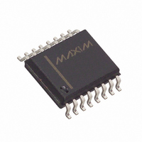
MAX520AEWE+ Maxim Integrated Products, MAX520AEWE+ Datasheet - Page 5

MAX520AEWE+
Manufacturer Part Number
MAX520AEWE+
Description
IC DAC 8BIT QUAD 2WIRE 16-SOIC
Manufacturer
Maxim Integrated Products
Datasheet
1.MAX520BCPE.pdf
(20 pages)
Specifications of MAX520AEWE+
Settling Time
2µs
Number Of Bits
8
Data Interface
I²C, Serial
Number Of Converters
4
Voltage Supply Source
Single Supply
Power Dissipation (max)
762mW
Operating Temperature
-40°C ~ 85°C
Mounting Type
Surface Mount
Package / Case
16-SOIC (0.300", 7.5mm Width)
Lead Free Status / RoHS Status
Lead free / RoHS Compliant
TIMING CHARACTERISTICS
(V
(V
Note 8: A master device must provide a hold time of at least 300ns for the SDA signal (referred to V
Note 9: Cb = total capacitance of one bus line in pF. t
Note 10: An input filter on the SDA and SCL input suppresses noise spikes less than 50ns.
Note 11: Guaranteed by design.
__________________________________________Typical Operating Characteristics
Serial Clock Frequency
Bus Free Time Between a STOP and a
START Condition
Hold Time, (Repeated) Start Condition
Low Period of the SCL Clock
High Period of the SCL Clock
Setup Time for a Repeated START Condition
Data Hold Time
Data Setup Time
Rise Time of Both SDA and SCL Signals, Receiving
Fall Time of Both SDA and SCL Signals, Receiving
Fall Time of SDA Transmitting (Note 6)
Setup Time for STOP Condition
Capacitive Load for Each Bus Line
Pulse Width of Spike Suppressed
DD
DD
10
= 5V ±10%, T
= 5V, DAC outputs unloaded, T
9
8
7
6
5
4
3
2
1
0
-60
SUPPLY CURRENT vs. TEMPERATURE
bridge the undefined region of SCL’s falling edge.
OPERATING MODE OR
SHUTDOWN MODE
-30
0
TEMPERATURE (°C)
A
PARAMETER
= T
_______________________________________________________________________________________
MAX520
30
MIN
60
to T
90
Quad/Octal, 2-Wire Serial 8-Bit DACs
MAX
120 150
, unless otherwise noted. Typical values are at T
A
= +25°C, unless otherwise noted.)
35
30
25
20
15
10
40
5
0
-60
SYMBOL
TEMPERATURE (SHUTDOWN MODE)
t
t
t
t
t
V
ONE REF INPUT DRIVEN
HD, DAT
HD, STA
SU, DAT
SU, STO
SU, STA
R
REFERENCE INPUT CURRENT vs.
t
REF
t
-30
f
t
HIGH
LOW
SCL
BUF
Cb
t
t
and t
t
t
SP
R
F
F
= 4V
0
TEMPERATURE (°C)
f
measured between 0.3V
with Rail-to-Rail Outputs
(Note 8)
(Note 9)
(Note 9)
I
(Notes 10, 11)
MAX520
30
SINK
60
CONDITIONS
≤ 6mA (Note 9)
90
120 150
A
= +25°C.)
DD
and 0.7V
20 + 0.1Cb
20 + 0.1Cb
20 + 0.1Cb
-10
-12
-14
-16
-18
-2
-4
-6
-8
MIN
2
0
100
1.3
0.6
1.3
0.6
0.6
0.6
0
0
0
1k
V
V
CENTERED AT 2.5V
DD
REF
IL
DD
REFERENCE VOLTAGE INPUT
= 5V
of the SCL signal) in order to
= 4Vp-p SINE WAVE
.
TYP
FREQUENCY RESPONSE
10k
FREQUENCY (Hz)
MAX520
100k
MAX
400
300
300
250
400
0.9
50
1M
UNITS
kHz
pF
µs
µs
µs
µs
µs
µs
ns
ns
ns
ns
µs
ns
10M
5


