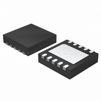
LTC2621CDD Linear Technology, LTC2621CDD Datasheet - Page 9

LTC2621CDD
Manufacturer Part Number
LTC2621CDD
Description
IC DAC 12BIT SGL R-R VOUT 10DFN
Manufacturer
Linear Technology
Datasheet
1.LTC2621CDDPBF.pdf
(16 pages)
Specifications of LTC2621CDD
Settling Time
7µs
Number Of Bits
12
Data Interface
Serial
Number Of Converters
1
Voltage Supply Source
Single Supply
Power Dissipation (max)
1.88mW
Operating Temperature
0°C ~ 70°C
Mounting Type
Surface Mount
Package / Case
10-DFN
Lead Free Status / RoHS Status
Contains lead / RoHS non-compliant
Available stocks
Company
Part Number
Manufacturer
Quantity
Price
Company:
Part Number:
LTC2621CDD
Manufacturer:
LT
Quantity:
10 000
Company:
Part Number:
LTC2621CDD#PBF
Manufacturer:
LTC
Quantity:
178
Company:
Part Number:
LTC2621CDD#TRPBF
Manufacturer:
RICOH
Quantity:
30 000
Company:
Part Number:
LTC2621CDD-1
Manufacturer:
LT
Quantity:
10 000
Company:
Part Number:
LTC2621CDD-1#PBF
Manufacturer:
LTC
Quantity:
378
TYPICAL PERFORMANCE CHARACTERISTICS
LTC2601/LTC2611/LTC2621
PIN FUNCTIONS
SDO (Pin 1): Serial Interface Data Output. This pin is used
for daisy-chain operation. The serial output of the shift
register appears at the SDO pin. The data transferred to
the device via the SDI pin is delayed 32 SCK rising edges
before being output at the next falling edge. SDO is an
active output and does not go high impedance even when
CS/LD is taken to a logic high level.
SDI (Pin 2): Serial Interface Data Input. Data is applied
to SDI for transfer to the device at the rising edge of SCK
(Pin 3). The LTC2601 accepts input word lengths of either
24 or 32 bits.
SCK (Pin 3): Serial Interface Clock Input. CMOS and TTL
compatible.
CLR (Pin 4): Asynchronous Clear Input. A logic low at this
level-triggered input clears all registers and causes the
DAC voltage outputs to drop to 0V for LTC2601/LTC2611/
LTC2621. A logic low at this input sets all registers to
midscale code and causes the DAC voltage outputs to go
to midscale for LTC2601-1/LTC2611-1/LTC2621-1. CMOS
and TTL compatible.
50
10
40
30
20
0
0
Short-Circuit Output Current vs
V
V
V
CODE = 0
V
OUT
CC
REF
OUT
= 5.5V
= 5.6V
SWEPT 0V TO V
(Sinking)
1
2
1V/DIV
3
CC
4
5
2601 G15
6
CS/LD (Pin 5): Serial Interface Chip Select/Load Input.
When CS/LD is low, SCK is enabled for shifting data on
SDI into the register. When CS/LD is taken high, SCK
is disabled and the specifi ed command (see Table 1) is
executed.
REF (Pin 6): Reference Voltage Input. 0V ≤ V
V
range is 0V to V
GND (Pin 8): Analog Ground.
V
LDAC (Pin 10): Asynchronous DAC Update Pin. If CS/LD
is high, a falling edge on LDAC immediately updates the
DAC register with the contents of the input register (similar
to a software update). If CS/LD is low when LDAC goes
low, the DAC register is updated after CS/LD returns high.
A low on the LDAC pin powers up the DAC. A software
power down command is ignored if LDAC is low.
Exposed Pad (Pin 11): Ground. Must be soldered to PCB
ground.
LTC2601/LTC2611/LTC2621
OUT
CC
(Pin 9): Supply Voltage Input. 2.5V ≤ V
(Pin 7): DAC Analog Voltage Output. The output
–10
–20
–30
–40
–50
0
0
Short-Circuit Output Current vs
V
V
V
CODE = FULL SCALE
V
OUT
CC
REF
OUT
= 5.5V
= 5.6V
SWEPT V
(Sourcing)
1
REF
.
2
CC
TO 0V
1V/DIV
3
4
5
2601 G16
6
CC
REF
≤ 5.5V.
≤ V
CC
2601fb
9
.


