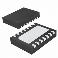
LTC2636IDE-LZ8#PBF Linear Technology, LTC2636IDE-LZ8#PBF Datasheet

LTC2636IDE-LZ8#PBF
Specifications of LTC2636IDE-LZ8#PBF
Available stocks
Related parts for LTC2636IDE-LZ8#PBF
LTC2636IDE-LZ8#PBF Summary of contents
Page 1
... L, LT, LTC, LTM, Linear Technology and the Linear logo are registered trademarks of Linear Technology Corporation. All other trademarks are the property of their respective owners. Protected by U.S. Patents including 5396245, 5859606, 6891433, 6937178, 7414561. ...
Page 2
LTC2636 ABSOLUTE MAXIMUM RATINGS Supply Voltage (V ) ................................... –0. CS/LD, SCK, SDI, LDAC, CLR ....................... –0. A–V H .................–0.3V to Min(V OUT OUT REF ...................................–0.3V to Min(V Operating Temperature Range LTC2636C ................................................ 0°C ...
Page 3
ORDER INFORMATION LTC2636 C DE – #TR Consult LTC Marketing for information on non-standard lead based fi nish parts. For more information on lead free part marking, go to: For more information on tape and reel specifi cations, ...
Page 4
LTC2636 PRODUCT SELECTION GUIDE PART MARKING PART NUMBER DFN MSOP REFERENCE LTC2636-LMI12 LMI12 6LMI12 2.5V•(4095/4096) LTC2636-LMI10 LMI10 6LMI10 2.5V•(1023/1024) LTC2636-LMI8 6LMI8 36LMI8 2.5V•(255/256) LTC2636-LMX12 LMX12 6LMX12 2.5V•(4095/4096) LTC2636-LMX10 LMX10 6LMX10 2.5V•(1023/1024) LTC2636-LMX8 6LMX8 36LMX8 2.5V•(255/256) LTC2636-LZ12 6LZ12 36LZ12 ...
Page 5
ELECTRICAL CHARACTERISTICS temperature range, otherwise specifi cations are at T LTC2636-LMI12/-LMI10/-LMI8/-LMX12/-LMX10/-LMX8/-LZ12/-LZ10/-LZ8 (V SYMBOL PARAMETER CONDITIONS DC Performance Resolution Monotonicity V = 3V, Internal Reference (Note 4) CC DNL Differential Nonlinearity V = 3V, Internal Reference (Note 4) CC INL Integral ...
Page 6
LTC2636 ELECTRICAL CHARACTERISTICS temperature range, otherwise specifi cations are at T LTC2636-LMI12/-LMI10/-LMI8/-LMX12/-LMX10/-LMX8/-LZ12/-LZ10/-LZ8 (V SYMBOL PARAMETER Reference Input V Input Voltage Range REF Resistance Capacitance I Reference Current, Power-Down Mode REF Reference Output Output Voltage Reference Temperature Coeffi cient Output Impedance ...
Page 7
TIMING CHARACTERISTICS range, otherwise specifi cations are LTC2636-LMI12/-LMI10/-LMI8/-LMX12/-LMX10/-LMX8/-LZ12/-LZ10/-LZ8 (V SYMBOL PARAMETER t1 SDI Valid to SCK Setup t2 SDI Valid to SCK Hold t3 SCK High Time t4 SCK Low Time CS/LD Pulse Width t5 LSB SCK ...
Page 8
LTC2636 ELECTRICAL CHARACTERISTICS temperature range, otherwise specifi cations are at T LTC2636-HMI12/-HMI10/-HMI8/-HMX12/-HMX10/-HMX8/-HZ12/-HZ10/-HZ8 (V SYMBOL PARAMETER V DAC Output Span OUT PSR Power Supply Rejection I Short Circuit Output Current (Note 6) SC Sinking Sourcing Power Supply V Positive Supply Voltage ...
Page 9
ELECTRICAL CHARACTERISTICS temperature range, otherwise specifi cations are at T LTC2636-HMI12/-HMI10/-HMI8/-HMX12/-HMX10/-HMX8/-HZ12/-HZ10/-HZ8 (V SYMBOL PARAMETER e Output Voltage Noise Density n Output Voltage Noise TIMING CHARACTERISTICS range, otherwise specifi cations are LTC2636-HMI12/-HMI10/-HMI8/-HMX12/-HMX10/-HMX8/-HZ12/-HZ10/-HZ8 (V SYMBOL PARAMETER t1 SDI Valid ...
Page 10
LTC2636 TYPICAL PERFORMANCE CHARACTERISTICS T = 25°C, unless otherwise noted. LTC2636-L12 (Internal Reference Integral Nonlinearity (INL) 1 0.5 0 –0.5 –1.0 0 1024 2048 CODE INL vs Temperature 1 INL ...
Page 11
TYPICAL PERFORMANCE CHARACTERISTICS T = 25°C, unless otherwise noted. LTC2636-H12 (Internal Reference Integral Nonlinearity (INL) 1 0.5 0 –0.5 –1.0 0 1024 2048 CODE INL vs Temperature 1 INL (POS) ...
Page 12
LTC2636 TYPICAL PERFORMANCE CHARACTERISTICS LTC2636-10 Integral Nonlinearity (INL) 1 2.5V FS INTERNAL REF . 0.5 0 –0.5 –1.0 0 256 CODE LTC2636-8 Integral Nonlinearity (INL) 0. 2.5V FS ...
Page 13
TYPICAL PERFORMANCE CHARACTERISTICS LTC2636 Large-Signal Response V OUT 0.5V/DIV 1/4 SCALE to 3/4 SCALE 2μs/DIV 2636 G22 Headroom at Rails vs Output Current 5.0 5V SOURCING 4.5 4.0 3.5 3V (LTC2636-L) SOURCING 3.0 ...
Page 14
LTC2636 TYPICAL PERFORMANCE CHARACTERISTICS LTC2636 Multiplying Bandwidth 2 0 –2 –4 –6 –8 –10 – – REF(DC 0.2V –16 REF(AC) P-P CODE = FULL-SCALE –18 1k 10k FREQUENCY (Hz) Gain Error ...
Page 15
PIN FUNCTIONS (DFN/MSOP) V (Pin 1/1): Supply Voltage Input. 2.7V ≤ (LTC2636-L) or 4.5V ≤ V ≤ 5.5V (LTC2636-H). Bypass CC to GND with a 0.1μF capacitor (Pins 2-5, 10-13/2-5, 12-15): DAC OUT ...
Page 16
LTC2636 BLOCK DIAGRAM GND V OUTA V REF V OUTB V REF V OUTC V REF V OUTD CS/LD SCK (LDAC) TIMING DIAGRAMS SCK SDI t 5 CS/LD LDAC 16 INTERNAL REFERENCE DAC A DAC B DAC C DAC D ...
Page 17
OPERATION The LTC2636 is a family of octal voltage output DACs in 14-lead DFN and 16-lead MSOP packages. Each DAC can operate rail-to-rail using an external reference, or with its full-scale voltage set by an integrated reference. Eighteen combinations of ...
Page 18
LTC2636 OPERATION INPUT WORD (LTC2636-12) COMMAND ADDRESS INPUT WORD (LTC2636-10) COMMAND ADDRESS INPUT WORD (LTC2636-8) COMMAND ADDRESS Serial Interface The CS/LD input is level triggered. ...
Page 19
OPERATION LTC2636 2636fb 19 ...
Page 20
LTC2636 OPERATION at the REF pin. Adding bypass capacitance to the REF pin will improve noise performance; and up to 10μF can be driven without oscillation. The REF output must be buffered when driving an external DC load current. Alternatively, ...
Page 21
OPERATION OUTPUT VOLTAGE 0V NEGATIVE INPUT CODE OFFSET (b) Figure 4. Effects of Rail-to-Rail Operation On a DAC Transfer Curve (Shown for 12 Bits). (a) Overall Transfer Function (b) Effect of Negative Offset for Codes Near Zero (c) Effect of ...
Page 22
LTC2636 PACKAGE DESCRIPTION 0.70 0.05 3.30 0.05 3.60 0.05 2.20 0.05 1.70 0.05 PACKAGE OUTLINE 0.25 0.05 0.50 BSC 3.00 REF RECOMMENDED SOLDER PAD PITCH AND DIMENSIONS APPLY SOLDER MASK TO AREAS THAT ARE NOT SOLDERED 0.889 0.127 (.035 .005) ...
Page 23
... Added details to Note 3 Revised Typical Applications circuit Information furnished by Linear Technology Corporation is believed to be accurate and reliable. However, no responsibility is assumed for its use. Linear Technology Corporation makes no representa- tion that the interconnection of its circuits as described herein will not infringe on existing patent rights. LTC2636 ...
Page 24
... LTC2636DE-LMI12 10 M1 LT1991 OUT DAC A DAC H REF 0.1μF DAC B DAC G –15V 11 DAC C DAC F 10 DAC D DAC E 14 GND 2636 TA02 Pins for Each DAC REF 2 C Interface LT 0610 REV B • PRINTED IN USA © LINEAR TECHNOLOGY CORPORATION 2008 ±5V OUT 2636fb ...


