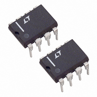
LTC1257CN8 Linear Technology, LTC1257CN8 Datasheet

LTC1257CN8
Specifications of LTC1257CN8
Available stocks
Related parts for LTC1257CN8
LTC1257CN8 Summary of contents
Page 1
... A when operating from a 5V supply, making the LTC1257 ideal for battery-powered applications. The space- saving 8-pin SO package and operation with no external components provide the smallest 12-bit D/A system available. , LTC and LT are registered trademarks of Linear Technology Corporation CLK P LOAD ...
Page 2
... REF 0 I 100 A REF V > 2.7V CC REF (Note 2) V Shorted to GND REF U W TOP VIEW ORDER PART NUMBER OUT LTC1257CN8 REF 6 LTC1257IN8 GND 5 N8 PACKAGE 8-LEAD PDIP = 100 C/W JA TOP VIEW LTC1257CS8 LTC1257IS8 V 7 OUT REF 6 S8 PART MARKING GND 5 1257 ...
Page 3
ELECTRICAL CHARACTERISTICS The denotes the specifications which apply over the full operating temperature range, otherwise specifications are 4.75V to 15.75V, internal or external reference (2.475V V A MIN MAX CC SYMBOL ...
Page 4
LTC1257 W U TYPICAL PERFOR A CE CHARACTERISTICS Minimum Supply Voltage vs Load Current #1 5 INTERNAL REF 4 FULL SCALE OUT 4.6 A 4.4 4.2 4.0 3.8 3.6 3.4 3.2 3.0 ...
Page 5
W U TYPICAL PERFOR A CE CHARACTERISTICS Differential Nonlinearity (DNL) 0.5 0.0 –0.5 0 512 1024 1536 2048 2560 3072 3584 4098 CODE 1257 TA05 CTIO S CLK (Pin 1): The TTL level input for ...
Page 6
LTC1257 U U DEFI ITIO S LSB: The least significant bit or the ideal voltage difference between two successive codes. n LSB = (V – V )/2 – The number of digital input bits V ...
Page 7
W BLOCK DIAGRA LOGIC SUPPLY CLK D IN LOAD REF DIAGRA t 1 CLK D IN MSB LOAD B11 D OUT (PREVIOUS WORD) 5V REGULATOR 12-BIT SHIFT REGISTER 12 12-BIT LATCH 12 2.048V REFERENCE ...
Page 8
LTC1257 U OPERATIO Serial Interface The data on the D input is loaded into the shift register IN on the rising edge of the clock. The MSB is loaded first and the LSB last. The DAC register loads the data ...
Page 9
U TYPICAL APPLICATIO S 5V 100 0.1 F 100k 2N3906 V IN – J LT1025A + GND COMMON + 10 F – 1k Auto Ranging 8-Channel ADC with Shutdown CH0 ANALOG • D ...
Page 10
LTC1257 PACKAGE DESCRIPTIO 0.300 – 0.325 (7.620 – 8.255) 0.009 – 0.015 (0.229 – 0.381) +0.035 0.325 –0.015 +0.889 8.255 –0.381 *THESE DIMENSIONS DO NOT INCLUDE MOLD FLASH OR PROTRUSIONS. MOLD FLASH OR PROTRUSIONS SHALL NOT EXCEED 0.010 INCH (0.254mm) ...
Page 11
... FLASH SHALL NOT EXCEED 0.010" (0.254mm) PER SIDE Information furnished by Linear Technology Corporation is believed to be accurate and reliable. However, no responsibility is assumed for its use. Linear Technology Corporation makes no represen- tation that the interconnection of its circuits as described herein will not infringe on existing patent rights. ...
Page 12
... Output Swings from GND to REF, REF Input Can Be Tied Output Swings from GND to REF, REF Input Can Be Tied Programmable Speed/Power, SO-8 Footprint (3V), Low Power, Deglitched 4.096V (0V to 2.5V) OUT 1257fb LT/TP 1101 REV B 1.5K • PRINTED IN USA LINEAR TECHNOLOGY CORPORATION 1994 ...


