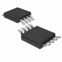
LTC2602CMS8 Linear Technology, LTC2602CMS8 Datasheet - Page 9

LTC2602CMS8
Manufacturer Part Number
LTC2602CMS8
Description
IC DAC 16BIT DUAL R-R VOUT 8MSOP
Manufacturer
Linear Technology
Datasheet
1.LTC2622IMS8PBF.pdf
(16 pages)
Specifications of LTC2602CMS8
Settling Time
10µs
Number Of Bits
16
Data Interface
Serial
Number Of Converters
2
Voltage Supply Source
Single Supply
Power Dissipation (max)
6.5mW
Operating Temperature
0°C ~ 70°C
Mounting Type
Surface Mount
Package / Case
8-MSOP, Micro8™, 8-uMAX, 8-uSOP,
Lead Free Status / RoHS Status
Contains lead / RoHS non-compliant
Available stocks
Company
Part Number
Manufacturer
Quantity
Price
Company:
Part Number:
LTC2602CMS8
Manufacturer:
LT
Quantity:
10 000
Part Number:
LTC2602CMS8
Manufacturer:
LINEAR/凌特
Quantity:
20 000
Part Number:
LTC2602CMS8#PBF
Manufacturer:
LINEAR/凌特
Quantity:
20 000
Part Number:
LTC2602CMS8#TRPBF
Manufacturer:
LINEAR/凌特
Quantity:
20 000
PIN
BLOCK DIAGRA
CS/LD (Pin 1): Serial Interface Chip Select/Load Input.
When CS/LD is low, SCK is enabled for shifting data on SDI
into the register. When CS/LD is taken high, SCK is dis-
abled and the specified command (see Table 1) is ex-
ecuted.
SCK (Pin 2): Serial Interface Clock Input. CMOS and TTL
compatible.
SDI (Pin 3): Serial Interface Data Input. Data is applied to
SDI for transfer to the device at the rising edge of SCK. The
TI I G DIAGRA
CS/LD
U
W
SCK
SDI
FUNCTIONS
U
U
t
5
V
CS/LD
U
OUT A
GND
SCK
7
1
2
8
W
W
DAC A
t
7
t
1
C3
t
2
1
CONTROL
C2
LOGIC
24-BIT SHIFT REGISTER
t
3
2
Figure 1
t
4
LTC2602/LTC2612/LTC2622 accept input word lengths
of either 24 or 32 bits.
REF (Pin 4): Reference Voltage Input. 0V ≤ V
V
Outputs. The output range is 0 – V
V
GND (Pin 7): Analog Ground.
OUT B
CC
DECODE
C1
(Pin 6): Supply Voltage Input. 2.5V ≤ V
3
LTC2602/LTC2612/LTC2622
and V
OUT A
D1
23
(Pins 5 and 8): DAC Analog Voltage
DAC B
D0
2602 BD
t
5
6
4
3
6
24
V
V
REF
SDI
OUT B
CC
REF
t
10
.
CC
REF
2602 F01
≤ 5.5V.
≤ V
2602fa
CC
9
.


