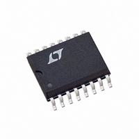
LTC1454CS Linear Technology, LTC1454CS Datasheet - Page 5

LTC1454CS
Manufacturer Part Number
LTC1454CS
Description
IC D/A CONV 12BIT R-R DUAL16SOIC
Manufacturer
Linear Technology
Datasheet
1.LTC1454CNPBF.pdf
(12 pages)
Specifications of LTC1454CS
Settling Time
14µs
Number Of Bits
12
Data Interface
Serial
Number Of Converters
2
Voltage Supply Source
Single Supply
Power Dissipation (max)
3.5mW
Operating Temperature
0°C ~ 70°C
Mounting Type
Surface Mount
Package / Case
16-SOIC (3.9mm Width)
Lead Free Status / RoHS Status
Contains lead / RoHS non-compliant
Available stocks
Company
Part Number
Manufacturer
Quantity
Price
Part Number:
LTC1454CS
Manufacturer:
LINEAR/凌特
Quantity:
20 000
Part Number:
LTC1454CS#TRPBF
Manufacturer:
LINEAR/凌特
Quantity:
20 000
PIN
X1/X2 B, X1/X2 A (Pins 1, 7): For LTC1454, when this pin
is grounded, the gain will be 2. When connected to V
the gain will be 1. In a gain of 2 configuration, the output
full scale will be 2
reference, this value is 4.096V. For the LTC1454L, when
this pin is grounded, the gain will be 2.05. When connected
to V
output full scale will be 2.05
internal reference this value is 2.5V.
CLR (Pin 2): The Clear Pin for the DAC. Clears both DACs
to zero scale when pulled low. This pin should be tied to
V
CLK (Pin 3): The Serial Interface Clock Input.
D
latched into the shift register on the rising edge of the serial
clock. Data is loaded as one 24-bit word. The first 12 bits
are for DAC A, MSB-first and the second 12 bits are for
DAC B, MSB-first.
CC
IN
U
OUT
(Pin 4): The Serial Data Input. Data on the D
for normal operation.
FUNCTIONS
the gain will be 1. In a gain of 2 configuration, the
U
U
REFHI. When using the internal
REFHI. When using the
IN
pin is
OUT
CS/LD (Pin 5): The Serial Interface Enable and Load
Control Input. When CS/LD is low the CLK signal is
enabled so the data can be clocked in. When CS/LD is
pulled high, data is loaded from the shift register into the
DAC register, updating the DAC output.
D
Becomes Valid on the Rising Edge of the Serial Clock.
V
V
quires a bypass capacitor to ground.
REFOUT (Pin 10): The Output of the Internal Reference.
REFHI A , REFHI B (Pins 11,14): The Inputs to the DAC
Resistor Ladder for DAC A/B.
REFLO (Pin 12): The Bottom of the DAC Resistor Ladder
for Both DACs. This can be used to offset zero-scale above
ground. REFLO should be connected to ground when no
offset is required.
GND (Pin 13): Ground.
OUT A,
CC
OUT
5.5V (LTC1454), 2.7V
(Pins 9, 15): The Positive Supply Input. 4.5
(Pin 6): The Output of the Shift Register which
V
OUT B
(Pins 8, 16): The Buffered DAC Outputs.
LTC1454/LTC1454L
V
CC
5.5V (LTC1454L). Re-
V
5
CC


