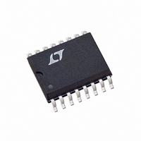
LTC1590IS Linear Technology, LTC1590IS Datasheet

LTC1590IS
Specifications of LTC1590IS
Available stocks
Related parts for LTC1590IS
LTC1590IS Summary of contents
Page 1
... Excellent accuracy, stability and versatility are combined with the smallest package available for a dual 12-bit multiplying DAC. Parts are available in 16-pin PDIP and narrow SO pack- ages and are specified over the commercial and industrial temperature ranges. , LTC and LT are registered trademarks of Linear Technology Corporation. 2 15V 33pF ® LT ...
Page 2
... To 0.01% for Full-Scale Change (Note 7) (Notes 5, 8) (Note 9) (Note 10) (Note 12 TOP VIEW ORDER PART NUMBER CLR LTC1590CN 3 14 CLK LTC1590CS LTC1590IN OUT LTC1590IS 6 11 CS/ DGND REF A S PACKAGE 16-LEAD PLASTIC SO = 150 C, = 100 C/W ( 150 C, = 150 C/W ( unless otherwise noted. MAX MIN TYP MAX 12 0.5 0 ...
Page 3
ELECTRICAL CHARACTERISTICS V = 4.5V to 5.5V 10V REF OUT1 SYMBOL PARAMETER Analog Outputs C Output Capacitance (Note 3) OUT Digital Input V Digital Input High Voltage IH V Digital Input Low Voltage IL ...
Page 4
LTC1590 W U TYPICAL PERFORMANCE CHARACTERISTICS Full-Scale Settling Waveform OUTPUT RANGE LT1363 OP AMP C 30pF FB TIME (500ns/DIV) 1590 G12 Multiplying Mode Signal-to- (Noise + Distortion) vs Frequency – ...
Page 5
W U TYPICAL PERFORMANCE CHARACTERISTICS Midscale Glitch Impulse LT1363 OP AMP C = 30pF FB TIME (500ns/DIV) 1590 G11 PIN FUNCTIONS (Pins 1, 9): Reference Inputs for DAC A/B. REF ...
Page 6
LTC1590 AGRA BLOCK V 1 REF B 40k DECODER D11 (MSB) LOAD V 9 REF A CS/LD 11 CLK TIMING DIAGRAMS OPERATING SEQUENCE DAC A INPUT MSB D D11 D10 ...
Page 7
TIMING DIAGRAMS TIMING DIAGRAM CLK D11 MSB CS/ D11 A D OUT PREVIOUS WORD U U APPLICATIONS INFORMATION Description The LTC1590 is a dual 12-bit multiplying DAC that ...
Page 8
LTC1590 U U APPLICATIONS INFORMATION Unipolar 2-Quadrant Multiplying Mode ( – OUT REF The LTC1590 can be used with a dual op amp to provide a dual 2-quadrant multiplying DAC as shown in Figure 2. ...
Page 9
U U APPLICATIONS INFORMATION Op Amp Selection To maintain the excellent accuracy and stability of the LTC1590 thought should be given to op amp selection. Fortunately, the sensitivity of INL and DNL to op amp offset has been significantly reduced ...
Page 10
LTC1590 U TYPICAL APPLICATIONS + V 3.3V 120k – LT1004-1.2 1/4 210k LT1179 + 0.1 F 50k 5V 0 DATA IN CLK 14 SERIAL CLOCK 11 CS/LD CHIP SELECT/DAC LOAD D 12 OUT DATA OUT ...
Page 11
... MOLD FLASH OR PROTRUSIONS SHALL NOT EXCEED 0.010 INCH (0.254mm) Information furnished by Linear Technology Corporation is believed to be accurate and reliable. However, no responsibility is assumed for its use. Linear Technology Corporation makes no represen- tation that the interconnection of its circuits as described herein will not infringe on existing patent rights. ...
Page 12
... S16 0695 15V 33pF 0. – 1 LT1358 OUT 16D V = –V OUT IN 4096 OUT A LT1358 6 – 4 0.01 F 33pF –15V 1590 TA10 1590f LT/TP 1197 4K • PRINTED IN USA LINEAR TECHNOLOGY CORPORATION 1997 ...


