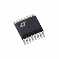
LTC2604CGN Linear Technology, LTC2604CGN Datasheet - Page 10

LTC2604CGN
Manufacturer Part Number
LTC2604CGN
Description
IC DAC 16BIT QUAD R-R OUT 16SSOP
Manufacturer
Linear Technology
Datasheet
1.LTC2624IGN-1PBF.pdf
(16 pages)
Specifications of LTC2604CGN
Settling Time
10µs
Number Of Bits
16
Data Interface
Serial
Number Of Converters
4
Voltage Supply Source
Single Supply
Power Dissipation (max)
10mW
Operating Temperature
0°C ~ 70°C
Mounting Type
Surface Mount
Package / Case
16-SSOP
Lead Free Status / RoHS Status
Contains lead / RoHS non-compliant
Available stocks
Company
Part Number
Manufacturer
Quantity
Price
Company:
Part Number:
LTC2604CGN
Manufacturer:
LT
Quantity:
10 000
Company:
Part Number:
LTC2604CGN-1
Manufacturer:
LT
Quantity:
10 000
LTC2604/LTC2614/LTC2624
TIMING DIAGRAM
OPERATION
Power-On Reset
The LTC2604/LTC2614/LTC2624 clear the outputs to
zero scale when power is fi rst applied, making system
initialization consistent and repeatable. The LTC2604-1/
LTC2614-1/LTC2624-1 set the voltage outputs to midscale
when power is fi rst applied.
For some applications, downstream circuits are active
during DAC power-up, and may be sensitive to nonzero
10
BLOCK DIAGRAM
CS/LD
SDO
SCK
SDI
REF LO
V
V
CS/LD
REF A
REF B
GND
SCK
OUTA
OUTB
1
2
3
4
5
6
7
8
t
5
DAC A
DAC B
t
7
t
1
t
2
1
CONTROL
LOGIC
32-BIT SHIFT REGISTER
Figure 1
t
3
2
t
8
outputs from the DAC during this time. The LTC2604/
LTC2614/LTC2624 contain circuitry to reduce the power-
on glitch; furthermore, the glitch amplitude can be made
arbitrarily small by reducing the ramp rate of the power
supply. For example, if the power supply is ramped to 5V
in 1ms, the analog outputs rise less than 10mV above
ground (typ) during power-on. See Power-On Reset Glitch
in the Typical Performance Characteristics section.
t
4
DECODE
3
23
DAC D
DAC C
t
6
24
V
V
REF D
REF C
2604 BD
OUT D
CLR
t
V
OUT C
SDO
SDI
10
16
15
14
13
12
11
10
CC
9
2604 F01
2604fd


