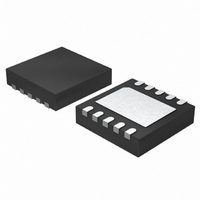
LTC2642AIDD-16#PBF Linear Technology, LTC2642AIDD-16#PBF Datasheet - Page 12

LTC2642AIDD-16#PBF
Manufacturer Part Number
LTC2642AIDD-16#PBF
Description
IC DAC 16BIT VOUT 10-DFN
Manufacturer
Linear Technology
Datasheet
1.LTC2642CDD-12PBF.pdf
(24 pages)
Specifications of LTC2642AIDD-16#PBF
Settling Time
1µs
Number Of Bits
16
Data Interface
Serial
Number Of Converters
1
Voltage Supply Source
Single Supply
Power Dissipation (max)
600µW
Operating Temperature
-40°C ~ 85°C
Mounting Type
Surface Mount
Package / Case
10-DFN
Lead Free Status / RoHS Status
Lead free / RoHS Compliant
Available stocks
Company
Part Number
Manufacturer
Quantity
Price
LTC2641/LTC2642
high-to-low transition, the data on DIN is loaded, MSB
fi rst, into the shift register on each rising edge of the serial
clock input (SCLK). After 16 data bits have been loaded
into the serial input register, a low-to-high transition on
CS transfers the data to the 16-bit DAC latch, updating
the DAC output (see Figures 1a, 1b, 1c). While CS remains
high, the serial input shift register is disabled. If there
are less than 16 low-to-high transitions on SCLK while
CS remains low, the data will be corrupted, and must be
reloaded. Also, if there are more than 16 low-to-high transi-
tions on SCLK while CS remains low, only the last 16 data
bits loaded from DIN will be transferred to the DAC latch.
For the 14-bit DACs, (LTC2641-14/LTC2642-14), the MSB
remains in the same (left-justifi ed) position in the input
16-bit data word. Therefore, two “don’t-care” bits must
be loaded after the LSB, to make up the required 16 data
bits (Figure 1b). Similarly, for the 12-bit family members
OPERATION
12
SCLK
SCLK
SCLK
DIN
DIN
DIN
CS
CS
CS
MSB
D15
MSB
MSB
D11 D10
D13
1
1
1
D14 D13 D12 D11 D10
D12 D11 D10
2
2
2
Figure 1a. 16-Bit Timing Diagram (LTC2641-16/LTC2642-16)
Figure 1b. 14-Bit Timing Diagram (LTC2641-14/LTC2642-14)
Figure 1c. 12-Bit Timing Diagram (LTC2641-12/LTC2642-12)
D9
3
3
3
D8
4
4
4
D7
D9
5
DATA (12 BITS + 4 DON’T-CARE BITS)
DATA (14 BITS + 2 DON’T-CARE BITS)
5
5
D6
D8
6
6
6
D9
DATA (16 BITS)
D5
D7
7
7
7
D8
D4
D6
8
8
8
D7
D3
D5
9
9
9
(LTC2641-12/LTC2642-12) four “don’t-care” bits must
follow the LSB (Figure 1c).
Power-On Reset
The LTC2641/LTC2642 include a power-on reset circuit
to ensure that the DAC ouput comes up in a known state.
When V
sets the output of the LTC2641 to zero-scale (code 0).
The LTC2642 powers up to midscale (bipolar zero). De-
pending on the DAC number of bits, the midscale code
is: 32,768 (LTC2642-16); 8,192 (LTC2642-14); or 2,048
(LTC2642-12).
Clearing the DAC
A 10ns (minimum) low pulse on the CLR pin asynchro-
nously clears the DAC latch to code zero (LTC2641) or to
midscale (LTC2642).
D6
D4
D2
10
10
10
D5
D1
D3
11
11
11
DD
D4
LSB
D0
D2
12
12
12
is fi rst applied, the power-on reset circuit
D3
D1
X
13
13
13
D2
LSB
D0
X
14
14
14
D1
X
X
15
15
15
LSB
D0
X
X
16
16
16
DAC
UPDATED
26412 F01a
DAC
UPDATED
26412 F01c
DAC
UPDATED
26412 F01b
26412fb


