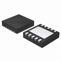
LTC2642AIDD-16#TRPBF Linear Technology, LTC2642AIDD-16#TRPBF Datasheet - Page 15

LTC2642AIDD-16#TRPBF
Manufacturer Part Number
LTC2642AIDD-16#TRPBF
Description
IC DAC 16BIT VOUT 10-DFN
Manufacturer
Linear Technology
Datasheet
1.LTC2642CDD-12PBF.pdf
(24 pages)
Specifications of LTC2642AIDD-16#TRPBF
Settling Time
1µs
Number Of Bits
16
Data Interface
Serial
Number Of Converters
1
Voltage Supply Source
Single Supply
Power Dissipation (max)
600µW
Operating Temperature
-40°C ~ 85°C
Mounting Type
Surface Mount
Package / Case
10-DFN
Lead Free Status / RoHS Status
Lead free / RoHS Compliant
Available stocks
Company
Part Number
Manufacturer
Quantity
Price
APPLICATIONS INFORMATION
Unbuffered Operation and V
The DAC output is available directly at the V
swings from GND to V
the lowest possible offset, full-scale and linearity errors, the
fastest settling time and minimum power consumption.
However, unbuffered operation requires that appropriate
loading be maintained on the V
LTC2642 V
in series with a source resistance of R
(Figure 4). The DAC’s linear output impedance allows it
to drive medium loads (R
or DNL; only the gain error is increased. The gain error
(GE) caused by a load resistance, R
scale) is:
In 16-bit LSBs:
R
independent of DAC code. The variation of R
part, is typically less than ±20%.
Note on LSB units:
For the following error descriptions, “LSB” means 16-bit
LSB and 65,536 is rounded to 66k.
To convert to 14-bit LSBs (LTC2641-14/LTC2642-14)
divide by 4.
To convert to 12-bit LSBs (LTC2641-12/LTC2642-12)
divide by 16.
A constant current, I
offset of:
For V
Since R
1LSB. Therefore, to avoid degrading DAC performance,
OUT
V
GE =
GE =
OFFSET
REF
has a low tempco (typically < ±50ppm/°C), and is
OUT
1+
1+
= 2.5V, a 16-bit LSB equals 2.5V/65,536, or 38μV.
–65536
OUT
= –I
is 6.2k, an I
–1
R
R
R
R
OUT
OUT
can be modeled as an ideal voltage source
L
L
L
• R
OUT
LSB
REF
L
, loading V
L
. Unbuffered operation provides
L
of 6nA produces an offset of
> 60k) without degrading INL
OUT
OUT
Loading
OUT
pin. The LTC2641/
OUT
L
, (relative to full
will produce an
, typically 6.2k
OUT
OUT
pin, which
, part-to-
it is critical to protect the V
leakage current.
Unbuffered V
The settling time at the V
mated by a single-pole response where:
(Figure 4). Settling to 1/2LSB at 16-bits requires about 12
time constants (ln(2 • 65,536)). The typical settling time
of 1μs corresponds to a time constant of 83ns, and a
total (C
capacitance, C
3pF corresponds to 1μs settling to 1/2LSB.
Op Amp Selection
The optimal choice for an external buffer op amp depends
on whether the DAC is used in the unipolar or bipolar
mode of operation, and also depends on the accuracy,
speed, power dissipation and board area requirements of
the application. The LTC2641/LTC2642’s combination of
tiny package size, rail-to-rail single supply operation, low
power dissipation, fast settling and nearly ideal accuracy
specifi cations makes it impractical for one op amp type
to fi t every application.
In bipolar mode (LTC2642 only), the amplifi er operates
with the internal resistors to provide bipolar offset and
scaling. In this case, a precision amplifi er operating from
dual power supplies, such as the the LT1678 provides the
±V
In unipolar mode, the output amplifi er operates as a unity
gain voltage follower. For unipolar, single supply applica-
tions a precision, rail-to-rail input, single supply op amp
τ = R
REF
V
LTC2641
LTC2642
REF
output range (Figure 3).
OUT
OUT
( )
CODE
2
N
+ C
• (C
Figure 4. V
OUT
–
+
L
OUT
) of about 83ns/6.2k = 13pF . The internal
OUT
GND
V
REF
R
REF
Settling Time
OUT
is typically 10pF, so an external C
+ C
LTC2641/LTC2642
OUT
L
C
)
V
OUT
OUT
OUT
Pin Equivalent Circuit
OUT
pin can be closely approxi-
pin from any sources of
R
L
C
L
26412 F04
I
L
V
0V TO V
OUT
15
REF
26412fb
L
of


