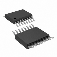
LTC2636IMS-LMX12#PBF Linear Technology, LTC2636IMS-LMX12#PBF Datasheet - Page 21

LTC2636IMS-LMX12#PBF
Manufacturer Part Number
LTC2636IMS-LMX12#PBF
Description
IC DAC 12-BIT OCTAL 16-MSOP
Manufacturer
Linear Technology
Datasheet
1.LTC2636IDE-HMI12PBF.pdf
(24 pages)
Specifications of LTC2636IMS-LMX12#PBF
Settling Time
4.4µs
Number Of Bits
12
Data Interface
MICROWIRE™, Serial, SPI™
Number Of Converters
8
Voltage Supply Source
Single Supply
Power Dissipation (max)
2.7mW
Operating Temperature
-40°C ~ 85°C
Mounting Type
Surface Mount
Package / Case
16-MSOP
Lead Free Status / RoHS Status
Lead free / RoHS Compliant
Available stocks
Company
Part Number
Manufacturer
Quantity
Price
OPERATION
Rail-to-Rail Output Considerations
In any rail-to-rail voltage output device, the output is lim-
ited to voltages within the supply range.
Since the analog output of the DAC cannot go below ground,
it may limit for the lowest codes as shown in Figure 4b.
Similarly, limiting can occur near full-scale when the REF
pin is tied to V
(FSE) is positive, the output for the highest codes limits
at V
occur if V
Offset and linearity are defi ned and tested over the region
of the DAC transfer function where no output limiting can
occur.
Board Layout
The PC board should have separate areas for the analog and
digital sections of the circuit. A single, solid ground plane
should be used, with analog and digital signals carefully
routed over separate areas of the plane. This keeps digital
signals away from sensitive analog signals and minimizes
the interaction between digital ground currents and the
analog section of the ground plane. The resistance from
NEGATIVE
OFFSET
CC
VOLTAGE
OUTPUT
, as shown in Figure 4c. No full-scale limiting can
0V
REF
is less than V
CC
. If V
Figure 4. Effects of Rail-to-Rail Operation On a DAC Transfer Curve (Shown for 12 Bits).
(a) Overall Transfer Function
(b) Effect of Negative Offset for Codes Near Zero
(c) Effect of Positive Full-Scale Error for Codes Near Full-Scale
REF
INPUT CODE
(b)
= V
CC
CC
–FSE.
and the DAC full-scale error
VOLTAGE
OUTPUT
0V
0
INPUT CODE
V
REF
2,048
(a)
= V
the LTC2636 GND pin to the ground plane should be as
low as possible. Resistance here will add directly to the
effective DC output impedance of the device (typically
0.1Ω). Note that the LTC2636 is no more susceptible to
this effect than any other parts of this type; on the con-
trary, it allows layout-based performance improvements
to shine rather than limiting attainable performance with
excessive internal resistance.
Another technique for minimizing errors is to use a sepa-
rate power ground return trace on another board layer.
The trace should run between the point where the power
supply is connected to the board and the DAC ground pin.
Thus the DAC ground pin becomes the common point for
analog ground, digital ground, and power ground. When
the LTC2636 is sinking large currents, this current fl ows
out the ground pin and directly to the power ground trace
without affecting the analog ground plane voltage.
It is sometimes necessary to interrupt the ground plane
to confi ne digital ground currents to the digital portion of
the plane. When doing this, make the gap in the plane only
as long as it needs to be to serve its purpose and ensure
that no traces cross over the gap.
CC
4,095
V
REF
INPUT CODE
= V
CC
(c)
LTC2636
2636 F04
OUTPUT
VOLTAGE
POSITIVE
FSE
21
2636fb


