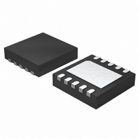
LTC2642CDD-16#PBF Linear Technology, LTC2642CDD-16#PBF Datasheet - Page 14

LTC2642CDD-16#PBF
Manufacturer Part Number
LTC2642CDD-16#PBF
Description
IC DAC 16BIT VOUT 10-DFN
Manufacturer
Linear Technology
Datasheet
1.LTC2642CDD-12PBF.pdf
(24 pages)
Specifications of LTC2642CDD-16#PBF
Settling Time
1µs
Number Of Bits
16
Data Interface
Serial
Number Of Converters
1
Voltage Supply Source
Single Supply
Power Dissipation (max)
600µW
Operating Temperature
0°C ~ 70°C
Mounting Type
Surface Mount
Package / Case
10-DFN
Number Of Channels
1
Resolution
16b
Interface Type
SER 3W SPI QSPI UW
Single Supply Voltage (typ)
3/5V
Dual Supply Voltage (typ)
Not RequiredV
Power Supply Requirement
Single
Output Type
Voltage
Integral Nonlinearity Error
±2LSB
Single Supply Voltage (min)
2.7V
Single Supply Voltage (max)
5.5V
Dual Supply Voltage (min)
Not RequiredV
Dual Supply Voltage (max)
Not RequiredV
Operating Temp Range
0C to 70C
Operating Temperature Classification
Commercial
Mounting
Surface Mount
Pin Count
10
Package Type
DFN EP
Lead Free Status / RoHS Status
Lead free / RoHS Compliant
Available stocks
Company
Part Number
Manufacturer
Quantity
Price
LTC2641/LTC2642
Bipolar Confi guration
Figure 3 shows a typical bipolar DAC application for the
LTC2642. The on-chip bipolar offset/gain resistors, R
and R
a bipolar output swing from –V
Table 2a. 16-Bit Bipolar Offset Binary
Code Table (LTC2642-16)
MSB
1111 1111 1111 1111 V
1000 0000 0000 0001 V
1000 0000 0000 0000 0V
0111 1111 1111 1111 –V
0000 0000 0000 0000 –V
APPLICATIONS INFORMATION
14
BINARY NUMBER
DIGITAL INPUT
IN DAC LATCH
INV
, are connected to an external amplifi er to produce
LSB
REF
REF
ANALOG OUTPUT
REF
REF
(32,767/32,768)
(1/32,768)
(1/32,768)
2
3
4
5
(V
CS
SCLK
DIN
CLR
OUT
LTC2642-16
)
Figure 3. 16-Bit Bipolar Output (LTC2642-16) V
REF
5V/3V
V
DD
9
to V
REF
0.1μF
16-BIT DAC
V
Table 2b. 14-Bit Bipolar Offset Binary
Code Table (LTC2642-14)
MSB
1111 1111 1111 11xx V
1000 0000 0000 01xx V
1000 0000 0000 00xx 0V
0111 1111 1111 11xx –V
0000 0000 0000 00xx –V
2.5V
at the R
REF
BINARY NUMBER
1
REF
DIGITAL INPUT
IN DAC LATCH
0.1μF
FB
pin.
GND
FB
V
R
INV
OUT
LSB
10
FB
4.7μF
8
7
6
26412 F02
The amplifi er circuit provides a gain of +2 from the V
pin, and gain of –1 from V
the bipolar offset binary code tables for 16-bit, 14-bit and
12-bit operation.
ANALOG OUTPUT
REF
REF
REF
REF
C1
10pF
OUT
(8,191/8,192)
(1/8,192)
(1/8,192)
(V
LT1019CS8-2.5
OUT
–
+
1/2 LT1678
GND
)
OUT
–5V
5V
= –V
IN
0.1μF
0.1μF
REF
5V
to V
Table 2c. 12-Bit Bipolar Offset Binary
Code Table (LTC2642-12)
MSB
1111 1111 1111 xxxx V
1000 0000 0001 xxxx V
1000 0000 0000 xxxx 0V
0111 1111 1111 xxxx –V
0000 0000 0000 xxxx –V
BIPOLAR V
–2.5V TO 2.5V
REF
BINARY NUMBER
DIGITAL INPUT
IN DAC LATCH
REF
. Tables 2a, 2b and 2c show
OUT
LSB
ANALOG OUTPUT
REF
REF
REF
REF
(2,047/2,048)
(1/2,048)
(1/2048)
(V
OUT
)
26412fb
OUT


